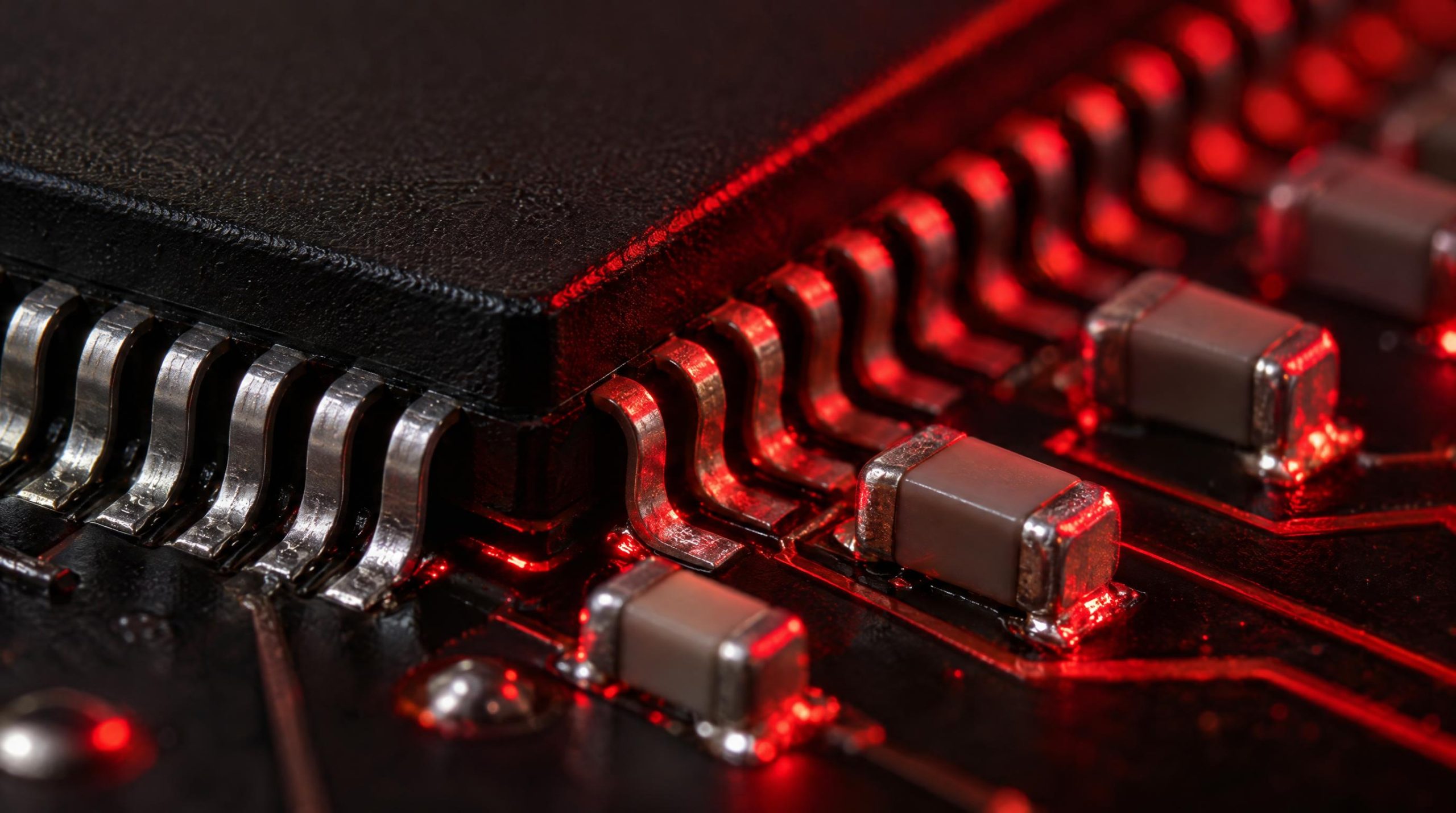
Open almost any PCB schematic and you will find small capacitors scattered between power pins and ground with no obvious signal function. They look like afterthoughts. They are not. These are decoupling capacitors, and their job is to keep integrated circuits alive when the power supply cannot react fast enough to a sudden current demand.
The concept sounds simple, but engineers routinely get it wrong — by using the wrong value for the frequency involved, by trusting a single capacitor to do work that requires three, or by placing a well-chosen component far enough from the IC that trace inductance cancels most of its benefit. This article works through all three questions — why decoupling capacitors are necessary, where they must be placed, and what value (and type) to select — with enough engineering depth to make the decisions stick.
Why Every IC Needs One · What Value to Choose · Where to Place It on Your PCB
● 5 Key Engineering Principles
|
⚡
Local Charge Reservoir Supplies current instantly when the regulator is too slow to react |
🎯
SRF Must Match Noise Above self-resonant frequency, the cap acts as an inductor — not a filter |
📈
Multi-Tier Strategy Layer different values to achieve continuous low-impedance coverage |
|
📍
Placement > Selection A well-chosen cap placed poorly will lose to an adequate cap placed correctly |
⚙
Dielectric Matters DC bias, temperature, and dielectric type can slash effective capacitance |
● Value Selection by Frequency
|
1–100µF Bulk / Low-Freq Electrolytic or large MLCC at power entry. Handles slow rail sag. |
1µF ~4 MHz SRF Mid-frequency bridge per power domain. |
STANDARD DEFAULT
100nF ~15 MHz SRF Per IC power pin. Handles most MCU transients up to ~16 MHz. |
|
10nF ~60 MHz SRF Supplements 100nF for fast switching ICs above 50 MHz. |
1nF ~500 MHz SRF GHz-range designs. Must be in tiny 0201 or 0402 package. |
| ⚠ |
Critical: Below the SRF a cap filters noise. Above it, the cap adds inductance. A 100nF cap on a 500 MHz path is not a filter — it is a problem. |
● Multi-Tier Decoupling Strategy
|
Tier 1 · Board Entry 100µF+ Bulk Electrolytic One per power entry point. Handles low-frequency rail droop from the supply. |
Tier 2 · Per Domain 1–10µF X7R MLCC One per power domain, near the IC cluster. Covers mid-frequency transitions. |
Tier 3 · Per Pin ★ 100nF X7R 0402 MLCC One per VCC power pin. Must be within 1–2mm of the IC. This is the most critical tier. |
● Dielectric Selection Guide
|
C0G / NP0 ✓
±0.3% over full temp range Zero DC bias effect. Best for PLL, RF, oscillators, precision analog. ⚠ Low density — impractical above ~10nF |
X7R DEFAULT
±15% | –55°C to +125°C Best all-rounder for power decoupling. Use 2–3× voltage rating to fight DC bias. ✓ Use as default for all digital rails |
|
X5R △
±15% | –55°C to +85°C Consumer electronics and room-temperature designs only. ⚠ Avoid in automotive / industrial |
Y5V ✕
Up to –80% capacitance loss Degrades severely with temperature and voltage. Nominal value is meaningless in-circuit. 🚫 AVOID for decoupling entirely |
| 💡 |
DC Bias Effect: A 10µF/10V X7R cap may deliver only 3–5µF when biased at 5V. Always derate: use a voltage rating of 2–3× the rail voltage to retain close to nominal capacitance. |
● PCB Placement Rules
|
Distance to Pin Place within 1–2mm of the IC power pin. Every extra millimeter of trace adds inductance and degrades performance. |
Routing Order Power must flow: Supply → Cap → IC Pin. Never route to the IC first and branch to the cap — that defeats local decoupling. |
|
Same-Layer Placement Keep caps on the same layer as the IC. Each via adds ~0.5–1nH of inductance per mm through the dielectric. |
Size Ordering Smallest cap closest to the IC for high-frequency transients. Larger bulk caps placed further away toward the power entry. |
| ⚠ |
Anti-Resonance: When mixing values in parallel, choose ratios >10× apart to avoid the high-impedance spike where the two capacitors’ inductances interact. Alternatively, parallel identical values — each divides total impedance without resonance peaks. |
● Package Size vs. ESL
| Package | Size (mm) | Package ESL | Best Use |
|---|---|---|---|
| 0201 | 0.6 × 0.3 | ~0.2–0.4 nH | GHz / RF designs |
| 0402 | 1.0 × 0.5 | ~0.4–0.8 nH | High-speed MCU / FPGA |
| 0603 | 1.6 × 0.8 | ~0.8–1.5 nH | Good balance / easy solder |
| 0805 | 2.0 × 1.25 | >1.5 nH | Hand-solder prototypes ≤80 MHz |
💡 Within any given package, inductance is set by geometry — not capacitance value. Always choose the highest capacitance available for your target package: you gain energy storage at zero inductance cost.
● Special Application Notes
|
♺ FPGAs Modern FPGAs have 3–6 separate power rails with different transient profiles. PLL and analog reference rails are the most sensitive — noise on these causes jitter. Use C0G ceramics (10nF + 100nF) for PLL supply bypass, plus a dedicated ferrite bead filter between the main rail and PLL pin. |
🎤 Analog / Op-Amp Circuits PSR in high-performance amplifiers degrades ~20 dB/decade with frequency — ~90 dB at DC but falls sharply. High-frequency rail noise couples directly to the output. Use a 100nF C0G for precision analog stages where X7R piezoelectric noise is a concern. |
● Quick-Reference Checklist
|
100nF X7R 0402 per VCC pin as default starting point Add 1–10µF mid-tier and 100µF+ bulk at power entry Verify cap value is capacitive at your circuit’s noise frequency Derate X7R voltage to 2–3× rail for accurate capacitance |
Place cap within 1–2mm of IC pin on the same PCB layer Route Supply → Cap → IC Pin (never branch off a main trace) Never use Y5V dielectric — capacitance collapses under bias and heat Qualify alternate part numbers across multiple MLCC vendors |
|
WIN SOURCE Global independent distributor of electronic components · win-source.net |
What Is a Decoupling Capacitor (and Why Does Every IC Need One)?
A decoupling capacitor acts as a localized energy reservoir for an integrated circuit (IC) on a printed circuit board (PCB). The core problem it solves is a timing mismatch: when a semiconductor switches states, it demands instantaneous current that the primary power supply cannot deliver fast enough — the physical traces between the voltage regulator and the IC carry parasitic inductance that resists rapid current changes — and the decoupling capacitor bridges this gap by supplying charge immediately from a source just millimeters away.
In practice, every digital IC and most analog ICs draw current in bursts. A microcontroller executing a tight loop, an FPGA reconfiguring its fabric, an op-amp driving a reactive load — all of them create momentary demands that the regulator, sitting some distance away on the board, cannot satisfy in time. Without a local charge reservoir, the supply voltage at the IC’s power pin dips, and those dips propagate as noise into every other circuit sharing the same rail. Professional PCB designs use multiple capacitors per power pin in parallel to achieve low impedance across a wide frequency range.
Decoupling vs. Bypass: Is There a Real Difference?
The two terms appear interchangeably in most documentation, and for good reason — both use identical physical components, typically multilayer ceramic capacitors (MLCCs), placed between a supply pin and ground. The conceptual distinction is directional: decoupling protects the IC from power supply sags; bypassing protects the power supply from noise generated by the IC.The difference lies in the functional intent you are designing for, and the loop dynamics you are analyzing, rather than the physical component you place.
For most design work, the distinction is academic. Select the right component, place it correctly, and it does both jobs simultaneously. The terminology matters more when reading application notes — a datasheet that says “bypass capacitor” and one that says “decoupling capacitor” are pointing to the same pad on the schematic.
The Physics Behind the Component: ESR, ESL, and Self-Resonant Frequency
A physical capacitor is modeled as a series RLC network consisting of Equivalent Series Resistance (ESR), Equivalent Series Inductance (ESL), and ideal capacitance (C). Each element limits performance in a different frequency range. ESR dissipates energy as heat and sets a floor on how low the capacitor’s impedance can fall. ESL determines the upper frequency limit: because of ESL, a capacitor reaches its minimum impedance at its self-resonant frequency (SRF), and above that point, inductive reactance dominates and blocks high-frequency filtering.
This is the single most important concept in decoupling design. Below the SRF, a component acts like a capacitor. Above it, it acts like an inductor. A 100 nF capacitor placed on a 500 MHz signal path is not providing any filtering — it is adding inductance. The capacitor you select must be capacitive at the frequencies your circuit actually generates, which requires knowing those frequencies before reaching for a component.
What Value to Use — And Why the Frequency of Noise Matters
Capacitance value and SRF are inversely related: larger capacitors resonate at lower frequencies, smaller ones at higher frequencies. As a rule of thumb for small SMD packages, a 1 µF capacitor resonates at roughly 4 MHz, a 100 nF capacitor at roughly 15 MHz, and a 10 nF capacitor at roughly 60 MHz — the exact figure depends on the package and the layout around it, so read the impedance curve for the specific part.
For general value guidance by noise frequency:
- Low-frequency noise (bulk stabilization):Values between 1 µF and 100 µF handle low-frequency noise decoupling.
- High-frequency transient suppression:High-frequency noise is addressed by values between 0.01 µF and 0.1 µF.
- Very high-speed ICs (100 MHz+):A 10 nF (0.01 µF) ceramic capacitor supplements the standard 100 nF for very high-speed ICs, since its higher SRF handles faster transients.
One important caveat applies to X7R and X5R dielectric capacitors used on power rails: a 10 µF / 10 V X7R capacitor may measure only 3–5 µF when biased at 5 V due to the ferroelectric polarization (DC bias) effect. This means a capacitor nominally rated at 10 µF may be delivering significantly less useful capacitance under operating conditions. For X7R decoupling capacitors on a supply rail, use a voltage rating of at least 2–3× the rail voltage to keep capacitance close to its nominal value.
The Multi-Tier Decoupling Strategy
No single capacitor value covers the full frequency range of a modern digital circuit. The practical approach is to layer capacitors of different values so their individual effective ranges overlap, forming a continuous low-impedance path from the low-frequency regime up through several hundred megahertz. To provide effective decoupling over a broader frequency range, incorporate capacitors with different values, such as 0.1 µF, 1 µF, and 10 µF.
A widely used tiered approach structures the decoupling network as follows:
- Local bypass (per power pin):One 100 nF ceramic per IC power pin handles most 8–16 MHz microcontroller designs adequately.
- Mid-frequency support:Adding a 100 nF ceramic with a 1 µF ceramic per power pin covers both high-frequency transients and lower-frequency bulk requirements, with the smaller cap placed closer to the pin.
- Board-level bulk:A three-tier arrangement of 10 nF + 100 nF + 10 µF per power domain, plus a 100 µF or larger bulk electrolytic at the power entry point, handles the full frequency spectrum from board entry through local transients.
One risk with mixing values is anti-resonance. When two capacitors of different values are placed in parallel, they can exhibit anti-resonance — a high-impedance peak at the frequency where their inductances interact — and the fix is to choose capacitor values far enough apart (more than a 10× ratio) while keeping physical placement close to minimize loop inductance differences between them. Alternatively, using multiple capacitors of the same type and value in parallel divides the total impedance by the number of capacitors and avoids the resonance peaks that arise from mixing different values.
Choosing the Right Dielectric: C0G, X7R, X5R, and What to Avoid
Ceramic capacitors dominate decoupling applications because of their low ESR and ESL, but the dielectric material inside the ceramic determines how the capacitor behaves under temperature, voltage, and frequency. The dielectric choice matters more than most datasheets make obvious.
C0G (NP0):C0G (NP0) is the most stable dielectric, with capacitance variation of ±0.3% maximum over the full temperature range, and it exhibits no DC bias effect.C0G capacitors have very low capacitance density, so trying to achieve 1 µF of C0G capacitance would require a physically massive and expensive component.Use C0G wherever stability matters — oscillators, PLL, RF, and precision circuits — and use X7R for general-purpose decoupling where high capacitance density is the priority.
X7R:X7R provides ±15% capacitance variation over –55°C to +125°C, making it suitable for general-purpose power decoupling. It is the standard workhorse choice for most decoupling applications from logic supplies to analog power rails. Rely on X7R as your default for power decoupling and general circuit design.
X5R:X5R has a narrower temperature range (–55°C to +85°C) with ±15% variation, typically used in consumer electronics where cost is a priority. It is suitable for room-temperature designs but should be avoided in automotive and industrial environments where temperatures regularly exceed 85°C.
Y5V:Avoid Y5V dielectric for decoupling — it degrades badly with temperature and voltage. A Y5V capacitor can lose over 80% of its rated capacitance at operating temperature and voltage, making its nominal value largely meaningless under real-world conditions.
Package Size and Loop Inductance
Package size directly controls ESL, and ESL directly controls SRF. Smaller SMD packages have lower parasitic inductance and higher SRF: the 0402 (1.0 × 0.5 mm) package offers the best SRF for high-speed designs, the 0603 (1.6 × 0.8 mm) offers a good balance of SRF and solderability, and the 0805 (2.0 × 1.25 mm) is easier to solder by hand with SRF still adequate for most MCU work up to 80 MHz.
The ESL contribution from the package itself is only part of the total inductance in the loop. The total ESL includes package ESL (fixed by body size: 0201 ≈ 0.2–0.4 nH, 0402 ≈ 0.4–0.8 nH, 0603 ≈ 0.8–1.5 nH), plus pad and trace inductance of 0.5–2 nH depending on trace length, plus via inductance of approximately 0.5–1 nH per via per millimeter of via length in the dielectric. These contributions add up. Because SRF falls with the square root of total inductance, adding a nanohenry or so of via and trace inductance to a small-package capacitor can cut its effective SRF by half or more.
One useful modern insight is that for SMD components, whenever possible, choose the largest capacitance value available for your chosen package size, because inductance is governed by package geometry, not by capacitance value. Two 0402 capacitors with different capacitance values carry nearly identical ESL — so there is no penalty to choosing the higher value within a given footprint.
Placement Rules That Actually Matter
Placement determines effectiveness far more than component selection. A textbook-perfect capacitor value placed poorly will underperform a merely adequate value placed correctly. The governing principle is simple: minimize loop inductance and high-frequency current path length.
Concrete placement rules for PCB layout:
- Distance to pin:The decoupling capacitor must be placed as close to the IC power pin as the PCB layout allows — ideally within 1–2 mm — because the connecting trace is a parasitic inductor, and every extra millimeter of trace adds inductance and degrades the capacitor’s effectiveness.
- Routing priority:The correct current path is power supply → decoupling capacitor → IC power pin. If the VCC trace routes to the IC first and then branches to the capacitor, the inductance of that branch defeats the purpose of local decoupling.
- Layer preference:Keep decoupling capacitors on the same layer as the IC whenever possible, or use very short, wide connections to minimize via inductance.
- Via configuration:Local bypass capacitors should be placed as close as possible to IC power pins and should connect directly to power and ground planes whenever possible.
- Per-rail independence:Ensure each power supply rail has its own set of decoupling capacitors, as different power rails may have different current demands and impedance requirements.
- Smaller value, closer placement:Place small, low-ESL capacitors (0201 or 0402) closest to the IC pins to handle high-frequency transients, and place larger bulk capacitors (0805 or 1210) slightly further away to handle lower-frequency energy demands.
A common layout error is placing capacitors wherever space allows rather than where the physics demands. Designers sometimes place decoupling caps at the board edge or away from the IC because there is room there — this completely defeats the purpose — the cap must be next to the IC it is decoupling.
Special Considerations: Analog Circuits, FPGAs, and High-Speed Designs
Analog circuits introduce an additional concern beyond transient current supply. The power supply rejection (PSR) of a high-performance amplifier deteriorates with frequency at around 20 dB/decade — around 90 dB at DC, the PSR drops rapidly at higher frequencies — which means high-frequency energy on the power line couples directly to the output, and avoiding that energy entry is obligatory. A well-placed 100 nF ceramic in X7R or C0G (for particularly noise-sensitive analog stages) handles this effectively for most op-amp and ADC applications.
FPGAs present a more demanding challenge. Modern FPGAs have three to six separate power rails — core voltage, I/O banks, auxiliary supplies, and PLL supplies — each with different transient current profiles and noise sensitivity, with the PLL and analog reference supplies being the most sensitive because noise on these rails directly degrades jitter performance and phase noise.For FPGA PLL supply pins, the decoupling strategy should use C0G/NP0 ceramics for the final bypass stage (10 nF and 100 nF values) to avoid the piezoelectric noise that X7R dielectrics can inject, combined with a dedicated small ferrite bead filter between the main rail and the PLL supply pin.
For high-speed designs operating into the GHz range, the impedance simulation approach becomes necessary. Use impedance simulation tools to check the power delivery network (PDN) frequency response if your design is safety-critical. Vendor simulation tools from Murata, TDK, and Kemet provide DC bias curves and impedance plots for specific part numbers under operating conditions — values that can differ substantially from the nominal datasheet figures.
Sourcing Decoupling Capacitors
Common MLCC values in 0402 or 0603 are made by many manufacturers and are usually straightforward to buy. Supply conditions for passives can shift quickly, however. MLCC shortages have historically been driven by capacity constraints at a small number of dominant ceramic manufacturers, and designs that rely on a single value or single source become vulnerable when allocation tightens.
Proactive supply chain management for passive components means qualifying alternative part numbers before a shortage hits, maintaining approved vendor lists that span multiple MLCC manufacturers, and monitoring lifecycle status for any part specified in a long-running production program. WIN SOURCE, a global independent distributor of electronic components, stocks ceramic capacitors across a broad range of values, dielectrics and package sizes, covering current-production parts as well as values that are hard to find, and supports shortage sourcing, lifecycle management and alternative solutions for situations where the originally specified part is constrained or end-of-life — engaged as ongoing procurement infrastructure, before a line-down event rather than after. Any alternate part proposed for an existing design should be approved by your own engineering team, since a matching footprint and nominal value does not guarantee matching DC-bias behavior, ESL or SRF.
Summary
Decoupling capacitors are not optional components. They are a required part of any power delivery network that feeds a switching IC, and their effectiveness depends on three decisions made together: choosing a value whose SRF matches the noise frequencies present in the circuit, selecting a dielectric that remains stable under the operating voltage and temperature, and placing the component with enough physical proximity to the IC that trace and via inductance do not erode the benefit. A 100 nF X7R MLCC in an 0402 package, placed within 1–2 mm of the IC power pin and connected cap-first on the VCC trace, is the correct starting point for most digital designs. From there, the multi-tier strategy — adding a 1–10 µF mid-frequency capacitor and a board-level bulk capacitor at the power entry — extends coverage across the full spectrum. The details covered here reflect current industry practice and apply whether the design involves a basic 8-bit microcontroller or a multi-rail FPGA with dedicated PLL supplies.
Frequently Asked Questions
What value should a decoupling capacitor be?
For most digital ICs the starting point is one 100 nF ceramic capacitor per power pin, because its self-resonant frequency sits in the tens of megahertz where typical logic transients live. Add a 1–10 µF capacitor per power domain for mid-frequency demand and a bulk capacitor at the power entry point for low-frequency droop, and add a 10 nF or 1 nF part next to the pin for very fast ICs. The right value is whichever is still capacitive at the noise frequency you actually have.
Is a decoupling capacitor the same as a bypass capacitor?
Physically, yes — the same MLCC between a supply pin and ground does both jobs. The terms describe intent: decoupling keeps the IC’s supply steady when it draws a burst of current, bypassing keeps the IC’s switching noise off the shared rail. Datasheets use the words interchangeably, and the placement rules are identical.
Why must the decoupling capacitor be so close to the IC?
Because the trace between the capacitor and the pin is a parasitic inductor, and inductance is what the capacitor is there to overcome. Every extra millimeter raises the loop inductance, lowers the effective self-resonant frequency and weakens the high-frequency response. Within 1–2 mm on the same layer, routed supply → capacitor → pin, is the target; the smallest, lowest-ESL capacitor goes nearest the pin.
Can I use a Y5V or Z5U capacitor for decoupling?
It is best avoided. Those dielectrics can lose most of their nominal capacitance at temperature extremes or under DC bias, so the value on the reel bears little relation to what the IC sees in service. X7R is the usual default for power decoupling; X5R is acceptable below 85°C; C0G is the choice for PLL, RF and precision analog supplies where stability matters more than density.
Why does my 10 µF X7R capacitor measure far less on the board?
DC bias. The ferroelectric ceramic in Class II dielectrics loses capacitance as voltage is applied, and a 10 µF part rated at 10 V can deliver only a fraction of that on a 5 V rail, with small case sizes affected most. Check the manufacturer’s DC bias curve for the specific part and choose a voltage rating two to three times the rail voltage to stay near the nominal value.
Part discontinued, obsolete or hard to find?
WIN SOURCE is a global independent distributor of electronic components, supporting component supply, shortage sourcing, lifecycle management and alternative solutions. Visual inspection, non-destructive testing and electrical testing are applied according to material risk, customer requirements and the applicable quality process, and orders are covered by the published return policy and a 3-year warranty on eligible components.
Stock and pricing are updated daily — search a part number or contact us for current availability, lead time and a quote.
© 2026 Win Source Electronics. All rights reserved. This content is protected by copyright and may not be reproduced, distributed, transmitted, cached, or otherwise used without the prior written permission of Win Source Electronics.