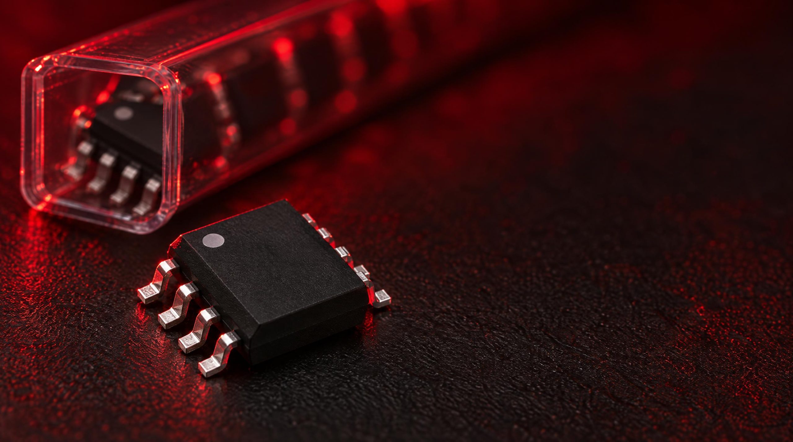
Memory ICs sit inside nearly every programmable system built in the last five decades — from microcontroller-based industrial sensors to server-grade computing platforms, from automotive ECUs to avionics computers still flying today. The four dominant families — SRAM, DRAM, EEPROM, and Flash — each evolved to solve a different combination of speed, density, power, and data-retention requirements. Understanding what differentiates them technically is useful. Understanding what happens to your supply chain when the specific density your design relies on reaches end-of-life (EOL) is critical.
This article covers both dimensions: the technical characteristics of each memory type, the architectural trade-offs that make each one suited to specific roles, and a practical look at the sourcing challenges that emerge when manufacturers retire older process nodes and density variants in favor of higher-capacity, more profitable products.
Architectures, applications, and supply-chain strategies for sourcing obsolete densities across all four memory families.
|
4
Memory Families
|
<5ns
SRAM Access Time
|
|
1M
EEPROM Endurance Cycles
|
10–20yr
Industrial Service Life
|
|
The Four Memory Families
|
|
SRAM
Static RAM
6-transistor bistable cell. No refresh needed. Fastest access times.
Volatile · Refresh-free
Access: <5 ns
Cost/bit: Highest
Unlimited write endurance
Used In
CPU cache, FPGAs, PLCs, medical devices, avionics
|
DRAM
Dynamic RAM
1T/1C capacitor cell. Every cell refreshed within a ~64 ms window.
Volatile · Refresh required
Access: ~50 ns (async)
Cost/bit: Low
High density
Used In
System RAM (DDR2–DDR5), servers, embedded PSRAM
|
|
EEPROM
Electrically Erasable PROM
2T floating-gate cell. Byte-level erase. High write endurance.
Non-volatile · Byte erase
Write cycle: ~5 ms
Up to 1,000,000 cycles
Low density (Kbit to low Mbit)
Used In
Calibration data, fault logs, odometer values, implants
|
Flash
NOR & NAND Flash
1T floating-gate. Block erase. NOR supports XIP; NAND is highest density.
Non-volatile · Block erase
Up to ~100,000 P/E cycles
Lowest cost/bit (NAND)
Very high density
Used In
Firmware storage (NOR), SSDs, eMMC, memory cards (NAND)
|
|
Application Verticals
|
|
Automotive
ECUs use NOR Flash for firmware, SRAM for runtime, EEPROM for fault codes. AEC-Q100 qualified. Lifecycles up to a decade.
|
Industrial
Systems stay validated for 10–20 years. Changing memory ICs triggers costly re-qualification. Obsolete parts are a recurring challenge.
|
|
✈️
Aerospace & Defense
Certification overhead can exceed part cost. Legacy SRAM and EEPROM variants affect airworthiness. Long program lifecycles demand exact part numbers.
|
Medical Devices
Regulatory validation ties designs to specific memory ICs. Component substitution may require re-submission to regulatory bodies.
|
|
5 Sourcing Strategies for Obsolete Memory ICs
|
|
|
|
|
|
|
5 Key Takeaways
|
|
▸
|
SRAM is fastest but costliest per bit — no refresh, unlimited write endurance, and access times under 5 ns make it irreplaceable for cache and deterministic low-latency applications.
|
|
▸
|
EEPROM’s byte-addressability is unique — no other mainstream non-volatile memory lets you update a single byte without erasing a large block, making it essential for frequently changing small data like calibration parameters.
|
|
▸
|
NOR Flash enables Execute-in-Place (XIP) — processors run code directly from the array, making NOR the firmware storage standard; NAND delivers maximum density but requires page-based access.
|
|
▸
|
Manufacturer economics ≠ your product lifecycle — as fabs consolidate around HBM and 3D NAND, legacy densities get discontinued regardless of how critical they are to your validated design.
|
|
▸
|
Proactive obsolescence management is a discipline — treating memory lifecycle risk as an ongoing procurement process, not a crisis response, preserves options and reduces emergency sourcing costs.
|
What Are Memory ICs?
A memory IC is a semiconductor device that stores binary data — strings of 1s and 0s — that a system can read, write, or both, depending on the memory type. At the circuit level, every memory array is a grid of storage cells, each capable of holding one or more bits. The cell design determines the speed, density, power consumption, volatility, and write endurance of the resulting device. The overarching classification most engineers use first is volatility: volatile memory requires a continuous power supply to retain its contents, while non-volatile memory preserves data through power-loss events indefinitely.
Within those two categories, SRAM and DRAM are the primary volatile technologies, and EEPROM and Flash occupy the non-volatile space alongside mask ROM and EPROM. Each type is also available across multiple interface variants — parallel, SPI, and I2C — which influences pin count, board complexity, and achievable data-transfer rates. The choice between them is rarely obvious; real designs often require more than one type on the same board.
SRAM: Fast, Refresh-Free, and Resource-Intensive
Static RAM (SRAM) stores each bit using a bistable flip-flop circuit — typically a six-transistor (6T) cell. The term “static” means the data state is held actively by the cross-coupled transistors as long as power is applied, with no need for periodic refresh cycles. That structural simplicity from a timing standpoint comes at a significant silicon cost: the 6T cell occupies many times the area of the one-transistor/one-capacitor cell used in DRAM. The result is lower storage density per die area and a substantially higher cost per bit.
In exchange, SRAM delivers access times that can fall below 5 nanoseconds — considerably faster than DRAM — and eliminates the controller complexity associated with refresh logic. Those properties make it the natural choice for processor cache memory, look-up tables in FPGAs, and high-speed data buffers in networking equipment. In embedded microcontrollers, small on-chip SRAM blocks serve as runtime working memory. Standalone external SRAM ICs, often in densities ranging from 256Kb to a few megabits, appear in industrial controllers, programmable logic controllers (PLCs), and medical devices where deterministic low-latency access is more important than raw capacity.
Battery-backed SRAM modules — which pair a standard SRAM die with an in-package lithium cell and control circuit — effectively convert volatile SRAM into a non-volatile storage element for applications requiring fast write cycles combined with data retention across power failures. These hybrid devices, and the specific density variants used in legacy industrial platforms, are among the harder-to-source memory ICs in the market today.
DRAM: High Density at Lower Cost
Dynamic RAM (DRAM) stores each bit as an electrical charge on a capacitor paired with a single access transistor — a one-transistor/one-capacitor (1T/1C) cell. This compact cell structure allows DRAM to achieve several times the density of SRAM for the same die area, and its cost-per-bit is substantially lower. Those two properties made DRAM the standard technology for main system memory in computers, workstations, and servers across several decades, evolving through SDRAM, DDR, DDR2, DDR3, DDR4, and DDR5 generations.
The trade-off is that the charge on each storage capacitor leaks away continuously, which means every cell must be refreshed — rewritten — within a fixed retention window, typically 64 milliseconds in modern DRAM, with refresh commands spread across that window. This periodic refresh requirement adds complexity to the memory controller, introduces brief periods of latency, and increases average power consumption. Typical DRAM access times are in the range of 50 nanoseconds for asynchronous variants, far slower than SRAM, though synchronous DRAM generations significantly reduced effective latency through burst-mode pipelines and higher clock rates.
Beyond standard DDR DIMMs, specialty DRAM variants — including pseudo-static DRAM (PSRAM), which integrates refresh logic on-chip to present an SRAM-like interface, and low-power LPDRAM families for mobile and embedded applications — are widely used in embedded systems. These specialty densities, particularly older asynchronous DRAM and early synchronous SDRAM parts, are frequently subject to discontinuation as manufacturers concentrate production capacity on high-volume DDR5 and High Bandwidth Memory (HBM) products.
EEPROM: Byte-Addressable Non-Volatile Storage
Electrically Erasable Programmable Read-Only Memory (EEPROM) is a non-volatile memory technology that can be erased and reprogrammed electrically, without the UV light exposure required by older EPROM devices. Its defining characteristic — the one that distinguishes it from Flash memory — is granularity: EEPROM supports erase and write operations at the byte or word level, rather than forcing the programmer to erase large blocks. That byte-addressability, combined with high endurance ratings that can reach one million program/erase cycles in modern devices, makes EEPROM the standard choice for storing small amounts of frequently updated non-volatile data: calibration parameters, configuration records, fault logs, odometer values, and similar application-specific data that changes often but in small increments.
The cost of that flexibility is low density and a relatively large cell structure. The programming circuits, charge-pump architecture, and double-polysilicon cell construction necessary for byte-level erasability require more silicon area per bit than Flash cells achieve. Serial EEPROM devices — accessed over I2C or SPI interfaces — typically range from 1 Kbit to a few megabits, which is adequate for parameter storage but impractical for firmware or bulk data. Parallel EEPROM variants exist in larger densities, though they are increasingly legacy products as Flash memory handles most larger non-volatile storage needs.
In microcontrollers, many vendors implement what they label “EEPROM” using a Flash array with firmware-level byte-erase emulation layered on top — a distinction that matters for write-endurance calculations and data retention planning in long-life products.
Flash Memory: NOR and NAND Architectures
Flash memory uses floating-gate transistors that trap electrons to represent stored data. Each program/erase cycle degrades the oxide layer surrounding the floating gate, which places a finite limit on write endurance — typically up to around 100,000 program/erase cycles for NOR Flash and SLC NAND, and considerably fewer for MLC, TLC and QLC NAND. The two dominant Flash architectures differ fundamentally in cell arrangement and access behavior, and that difference determines which applications each serves.
NOR Flash connects each cell to the bit line individually, enabling true random byte-level read access. This architecture supports Execute-in-Place (XIP) operation, where a processor executes code directly from the Flash array without copying it to RAM first. NOR is the preferred technology for firmware storage in embedded systems: boot code, application images, and other relatively static but executable content. Read performance is fast; write performance is moderate; and the block-erase requirement (typically 64KB to 128KB sectors) means NOR is poorly suited for frequent small writes. Density tops out at a few gigabits for standalone parts, and memory manufacturers routinely retire older low-density NOR parts as process nodes advance.
NAND Flash organizes cells in series strings, achieving a much higher cell density than NOR at lower cost per bit, but sacrificing random-access read capability. All reads and writes operate on page and block boundaries, which makes NAND unsuitable for XIP but ideal for mass data storage: SSDs, eMMC, memory cards, and USB drives. NAND has evolved from single-level cell (SLC) through MLC, TLC, and QLC to 3D-stacked architectures that push storage capacity to unprecedented levels, while simultaneously reducing per-byte cost. Older 2D (planar) NAND densities — SLC and MLC variants used in automotive, industrial, and aerospace embedded systems — are now being discontinued as manufacturers shift production toward 3D NAND.
Comparing the Four Memory Types
The table below summarizes the key technical trade-offs across the four memory families:
| Property | SRAM | DRAM | EEPROM | Flash (NOR/NAND) |
|---|---|---|---|---|
| Volatility | Volatile | Volatile | Non-volatile | Non-volatile |
| Cell structure | 6T flip-flop | 1T + 1 capacitor | 2T floating gate | 1T floating gate |
| Requires refresh | No | Yes (~64 ms window) | No | No |
| Typical access time | <5 ns | ~50 ns (async) | ~5 ms write cycle (byte/page) | NOR: ~70–100 ns read; NAND: page-based |
| Write endurance | Unlimited | Unlimited | ~1,000,000 cycles | Up to ~100,000 cycles (NOR, SLC NAND) |
| Relative density | Low | High | Low | Very high (NAND) |
| Cost per bit | Highest | Low | High | Lowest (NAND) |
| Byte-level erase | N/A | N/A | Yes | No (block erase) |
Application Verticals and Memory Selection
Memory selection is always context-driven. The same general rules apply broadly, but the weighting of each criterion shifts significantly from one vertical to another.
In automotive electronics, ECUs use NOR Flash for firmware storage and SRAM for runtime operations, with EEPROM dedicated to fault code logs and calibration data. Automotive-grade parts carry qualification standards such as AEC-Q100 and must operate across wide temperature ranges, typically -40°C to +125°C. Infotainment systems require higher-capacity DDR memory for UI rendering and NAND for map and media storage. The qualification overhead means design teams often continue using specific part numbers for the full vehicle program lifecycle — sometimes a decade or longer — and discontinuation of even a minor density variant can disrupt production.
In industrial and process control environments, once a control system is validated for a task — managing a power grid, coordinating an automated assembly line, or monitoring a chemical process — changing the hardware introduces significant risk and re-qualification cost. Industrial systems regularly remain in service for 10, 15, or 20 years. The memory ICs specified during the original design may have gone through two or three EOL cycles at the silicon vendor by the time a repair or retrofit is needed.
In aerospace and defense, the challenge is amplified further. Long program lifecycles and rigorous certification standards mean that replacing a memory component is rarely as straightforward as selecting a newer part number. The qualification effort for a flight-critical design can cost more than the components themselves, which means legacy part availability directly affects system airworthiness and program continuity. Mission-critical systems in avionics, communications, and defense electronics often depend on SRAM densities and EEPROM variants that left volume production years ago.
In medical devices, data integrity and traceability requirements make arbitrary component substitution impractical. The firmware stored in a NOR Flash device and the patient data written to EEPROM in an implantable or diagnostic instrument are subject to regulatory validation. A component change typically requires documentation, testing, and in some cases re-submission to regulatory bodies — so keeping the original memory IC in production is strongly preferred over redesign.
When the Density You Need Goes End-of-Life
Memory manufacturers operate on economics, not application lifecycles. As process nodes advance and production capacity is redirected toward higher-margin, higher-density products — HBM for AI accelerators, 3D NAND for enterprise SSDs — the older density variants that industrial and embedded systems depend on become commercially unattractive to produce. A manufacturer may issue a Product Change Notice (PCN) or Last Time Buy (LTB) notice for a 256Kx8 SRAM, a 1Mbit parallel EEPROM, or a 16Mbit NOR Flash part, giving customers a finite window to place final production orders before supply permanently ceases.
The core problem is lifecycle misalignment. The technology has not failed; the system that depends on it has not failed; but the supply chain infrastructure supporting that specific memory density has been discontinued. For an aerospace program or a medical instrument with a 20-year field life, an LTB notice issued five years into production leaves a 15-year sourcing gap that cannot simply be bridged by switching to the next-generation part. Replacing a single obsolete IC can trigger a cascade of consequences: board redesign, firmware modification, re-qualification testing, and regulatory re-submission — each step representing months of engineering time and significant cost.
The sourcing challenge is also compounded by counterfeit risk. As legitimate supply of a discontinued memory part dwindles, the market for remarked or recycled components expands. Parts sold as new may carry fraudulent date codes or have been harvested from used circuit boards. For safety-critical applications, the consequences of deploying a counterfeit or degraded memory IC can range from intermittent data corruption to catastrophic system failure. Authentication, quality inspection, and supply-chain traceability become essential procurement requirements, not optional extras.
Sourcing Strategies for Obsolete Memory ICs
There is no single universal approach to managing obsolete memory ICs, but effective supply-chain planning generally involves a combination of proactive and reactive strategies.
- Lifecycle monitoring: Track PCN and EOL notices from memory manufacturers. Acting on an LTB opportunity — placing a strategic buffer buy before last shipment dates — is far less disruptive than discovering a stockout mid-production. Monitoring services and distributor-managed alerts can automate this tracking for large BOMs.
- Bridge inventory: When an EOL notice is received with adequate lead time, securing a multi-year supply of the affected memory density allows production to continue while an engineering team evaluates longer-term migration options without deadline pressure.
- Form-fit-function alternatives: In some cases, a pin-compatible memory IC from a different manufacturer offers a direct drop-in replacement. Functional and electrical verification is still required, but the board layout and firmware remain unchanged. Identifying qualified alternatives before a shortage occurs is part of proactive obsolescence management.
- Locating remaining stock: Once a memory IC is past last-time-ship, purchasable stock can still exist across a number of supply channels, and locating it becomes a sourcing exercise rather than a catalog order.
- Supplier due diligence: What decides whether that stock is safe to buy is how the supplier manages quality, and the questions worth asking are the same whoever is quoting: which certifications it holds, how its counterfeit-mitigation process works, whether it is a member of ERAI, and what its inspection, date-code and return policies are. Match the depth of inspection to the risk the application carries.
For organizations managing complex BOMs across multiple product generations, the most effective approach treats memory component lifecycle risk as an ongoing procurement discipline rather than an incident-response exercise. Knowing which SRAM densities in your design are already in their last process node generation, which EEPROM variants have had a PCN filed in the last 12 months, and which legacy NAND parts your contract manufacturer is still able to source — that situational awareness is the foundation of supply-chain resilience for memory-dependent products.
WIN SOURCE is a global independent distributor of electronic components, founded in 1999, supporting component supply, shortage sourcing, lifecycle management and alternative solutions — covering current-production memory ICs across SRAM, DRAM, EEPROM, NOR and NAND Flash as well as densities that are hard to find, with verified stock and cross-reference support. It holds AS9120, ISO 9001:2015 and ISO 14001 certifications and is a member of ERAI. Where a drop-in replacement is proposed, final approval of the substitute rests with the customer’s engineering team.
Conclusion
SRAM, DRAM, EEPROM, and Flash memory ICs each occupy a distinct position in embedded and electronics design, defined by their cell architecture, speed, density, volatility, and write endurance. Selecting the right type for a given application is a technical exercise that most experienced engineers handle well. The harder problem — one that grows more acute as systems age and memory manufacturers consolidate around fewer, larger-density process nodes — is maintaining access to the specific parts a validated, certified, or safety-critical design depends on.
Proactive lifecycle monitoring, strategic buffer buys, alternative part qualification, and partnerships with capable independent distributors together form a supply-chain strategy that keeps obsolete memory densities from becoming production-halting crises. The earlier those measures are in place, the more options remain available.
Frequently Asked Questions
What is the difference between SRAM and DRAM?
SRAM stores each bit in a six-transistor flip-flop that needs no refresh and gives very fast access, at a high cost per bit. DRAM stores each bit as charge on a capacitor with one transistor, so it is far denser and cheaper per bit, but every cell must be refreshed periodically and access is slower.
When should I use EEPROM instead of Flash?
Use EEPROM for small amounts of data that change often — calibration constants, configuration records, fault logs — because it can be erased and rewritten a byte at a time with high endurance. Use Flash for firmware and bulk data, where block erase is acceptable and density and cost per bit matter more.
What is the difference between NOR and NAND Flash?
NOR Flash offers random byte-level reads and supports execute-in-place, which makes it the usual choice for boot code and firmware. NAND Flash reads and writes by page and erases by block, trading random access for much higher density and lower cost per bit, which suits SSDs, eMMC and memory cards.
Why do older memory densities go end-of-life?
Manufacturers move capacity to newer process nodes and higher-density, higher-margin products, so low-density SRAM, parallel EEPROM, small NOR Flash and planar NAND parts become uneconomic to keep producing even when fielded systems still depend on them.
How do I source a memory IC that has been discontinued?
Check for an open last-time-buy window first, then evaluate pin-compatible alternatives and locate remaining stock of the original with full traceability and inspection matched to the application’s risk. Any substitute needs functional and electrical verification, and final approval rests with the customer’s engineering team.
Part discontinued, obsolete or hard to find?
WIN SOURCE is a global independent distributor of electronic components, supporting component supply, shortage sourcing, lifecycle management and alternative solutions. Visual inspection, non-destructive testing and electrical testing are applied according to material risk, customer requirements and the applicable quality process, and orders are covered by the published return policy and a 3-year warranty on eligible components.
Stock and pricing are updated daily — search a part number or contact us for current availability, lead time and a quote.
© 2026 Win Source Electronics. All rights reserved. This content is protected by copyright and may not be reproduced, distributed, transmitted, cached, or otherwise used without the prior written permission of Win Source Electronics.