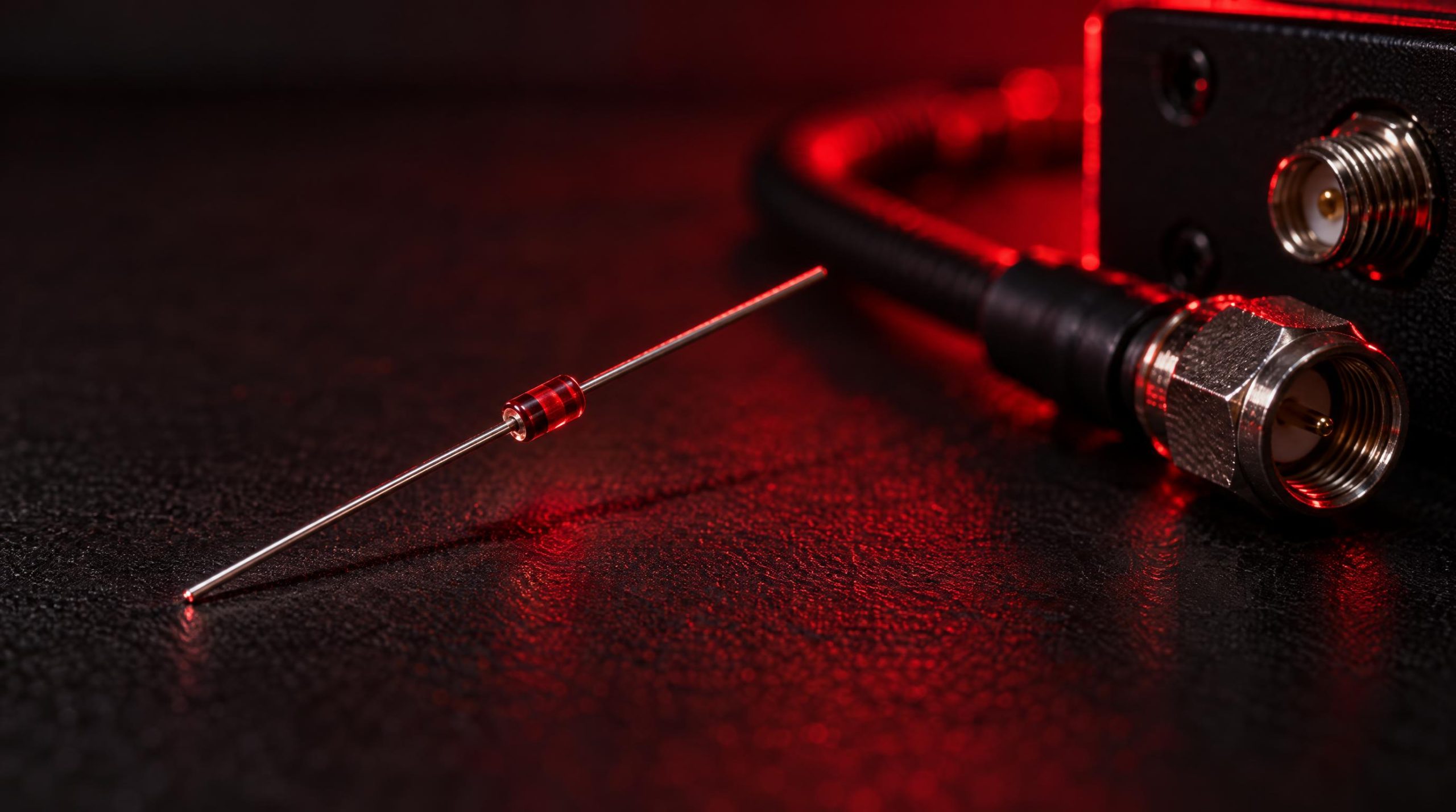
The PIN diode is one of those components that looks unremarkable on a schematic but does something mechanically elegant at the physics level. It is a three-layer semiconductor device — P-type, Intrinsic, N-type — and that extra undoped middle layer transforms what would otherwise be a conventional rectifier into a precision-controlled RF element. Engineers working in RF and microwave design rely on it for signal routing, power leveling, and protection, and it shows up in everything from base station front ends to radar transmit/receive modules to fiber-optic receivers.
This article explains the PIN diode from the ground up: its structure, the physics behind its high-frequency behavior, how it functions as both a switch and a continuously variable attenuator, the common circuit topologies used in real designs, and what to look for when selecting one for a specific application.
How a three-layer semiconductor transforms RF switching, attenuation, and signal control across telecommunications, radar, and fiber-optic systems.
|
3 layers
P–I–N structure: the intrinsic layer is the key
|
~0.1 Ω
On-state resistance at 100 mA bias
|
|
10 kΩ+
Off-state resistance at near-zero bias
|
< 1pF
Typical Off-State Capacitance
|
|
What Is a PIN Diode?
|
|
P⁺ P-Type
Holes (majority carriers) |
KEY LAYER
I Intrinsic |
N⁺ N-Type
Electrons (majority carriers) |
The Positive–Intrinsic–Negative structure distinguishes the PIN diode from conventional PN junction diodes. The extra undoped middle layer transforms what would otherwise be a standard rectifier into a precision-controlled RF element capable of operating as a bias-controlled resistor across several orders of magnitude.
|
How It Works: Bias-Controlled RF Resistance
|
|
Forward Bias — ON State
|
Reverse Bias — OFF State
|
Key Insight: At high RF frequencies, the PIN diode appears as a resistor, not a nonlinear device. The RF waveform alternates faster than the carrier recombination time in the I-layer — so impedance is set entirely by the DC bias current, producing no rectification or distortion.
|
RF Switching Topologies
|
|
Series Topology
Diode in signal path. Forward bias = low resistance, signal passes. Reverse bias = high impedance, signal blocked. Off-state isolation limited by residual capacitance. |
Shunt Topology
Diode from signal line to ground. ON state short-circuits signal to ground (block). OFF state: high impedance, minimal effect. Better isolation at high frequencies. |
|
Series-Shunt (T/Pi)
Combines both approaches. Achieves low insertion loss in pass state AND high isolation in block state simultaneously. Standard for T/R switch designs. |
T/R Switch Use Case: In radar and transceiver systems, a single antenna switches between transmitter (TX) and receiver (RX) in microseconds while handling hundreds of watts on TX — PIN diodes enable this with complementary bias switching and nanosecond response times.
|
Variable Attenuation: Continuous RF Control
|
|
~10 kΩ Near-zero bias
|
~1 kΩ Low bias
|
~100 Ω Moderate
|
~10 Ω Higher bias
|
~0.1 Ω 100 mA
|
|
AGC Circuits
Attenuator placed before low-noise amplifier. Feedback loop adjusts PIN diode bias to maintain optimal signal level at amplifier input regardless of incoming signal strength. |
Radar Receiver Protection
Attenuator responds fast enough to prevent sensitive receiver front-end from being overloaded by strong reflected signal immediately after the transmit pulse. |
|
Key Application Areas
|
|
RF Switching
Telecom & radar signal routing |
Variable Attenuation
AGC & power leveling |
Radar T/R Modules
High-speed TX/RX switching |
|
Fiber Optics
High-speed photodetection |
RF Limiting
Front-end protection |
Medical Imaging
Rapid RF signal switching |
|
Selection Parameters Cheat Sheet
|
|
I-Layer Thickness (Wᵢ)
Thicker = higher VBR & power, slower switching. Thinner = faster, lower power floor.
|
Carrier Lifetime (τ)
Must be much longer than RF period. Short τ = nonlinear behavior at lower frequencies.
|
Series Resistance (Rₛ)
ON-state resistance at given bias. Directly sets switch insertion loss.
|
|
Junction Capacitance (Cⱼ)
OFF-state capacitance limits isolation at high frequencies. Lower = better for wideband.
|
Power Handling
Set by thermal resistance & I-layer geometry. Match to peak RF power in application.
|
Package Type
SMD (SOD-323, SOT-23) or chip/wire for MMIC. Account for package parasitics at mm-wave.
|
|
PIN Diode vs. Other RF Switch Technologies
|
| Technology | Power Handling | Insertion Loss | Speed | Linearity |
|---|---|---|---|---|
| PIN Diode | ★★★★☆ | ★★★★★ | ★★★★☆ | ★★★★★ |
| GaAs pHEMT FET | ★★★☆☆ | ★★★☆☆ | ★★★★★ | ★★★☆☆ |
| Electromechanical Relay | ★★★★★ | ★★★★★ | ★☆☆☆☆ | ★★★★★ |
|
5 Key Takeaways
|
| 01 |
The intrinsic layer is the defining feature — it enables linear RF resistance control and suppresses nonlinearity at high frequencies that would plague standard PN diodes. |
| 02 |
PIN diodes function as bias-controlled resistors — resistance spans from ~0.1 Ω to 10 kΩ, enabling both hard switching and smooth analog attenuation from the same device. |
| 03 |
I-layer thickness is the primary design trade-off: thicker improves breakdown voltage and power handling; thinner enables faster switching and lower on-state resistance. |
| 04 |
For T/R switches and radar front ends, PIN diodes outperform FETs in power handling and linearity, despite requiring more complex dual-rail bias circuitry. |
| 05 |
Sourcing specific RF PIN diode variants — especially military/space-qualified parts — requires a proactive supply chain strategy; many are lifecycle-sensitive and not interchangeable without full electrical re-verification. |
|
WIN SOURCE
Global Independent Electronic Components Distributor
|
|
What Is a PIN Diode?
A PIN diode is a semiconductor diode that includes an undoped (or very lightly doped) intrinsic semiconductor region sandwiched between a heavily doped P-type layer and a heavily doped N-type layer. The name is simply an acronym for the layer sequence: Positive–Intrinsic–Negative. This arrangement distinguishes it structurally and functionally from a standard PN junction diode, which has no such intermediate layer. While a conventional diode’s primary job is rectification, the PIN diode’s intrinsic layer makes it less useful as a rectifier but exceptionally well-suited for controlled impedance applications at radio and microwave frequencies.
The device is widely deployed, and much of the demand is driven by telecommunications infrastructure, satellite systems, and defense electronics — all domains where clean, high-speed RF switching and attenuation are critical requirements.
Structure and the Role of the Intrinsic Layer
The three regions of a PIN diode each have a distinct function. The P-type region is doped with acceptor impurities, providing holes as majority carriers; the intrinsic (I) region is a wide, undoped layer that increases the depletion region width; and the N-type region is doped with donor impurities, providing electrons as majority carriers. In practice, achieving a truly intrinsic (zero-doped) layer during fabrication is difficult, so the I-layer is typically very lightly doped — often in the range of roughly 1,000 ohm-cm resistivity — but the term “intrinsic” has stuck as a descriptor of the region’s behavior rather than its precise doping level.
The intrinsic layer is the most important part of the PIN diode because it modifies the electrical behavior, especially at high frequencies. Its thickness is a key design variable: a thicker I-layer increases the breakdown voltage and improves high-power handling, but it also raises the carrier transit time, which limits the upper frequency at which the device switches cleanly. A thinner I-layer reduces on-state resistance and enables faster switching, but lowers the power-handling ceiling. This trade-off means that PIN diodes used in low-frequency high-power transmitters look physically different from those used in millimeter-wave attenuators — the geometry is tuned to the application.
PIN diodes are manufactured using two main construction approaches, mesa and planar. In the mesa structure, pre-doped layers are added to the substrate, allowing control over the doping level and layer thickness. The Planar structure involves growing an epitaxial layer on the substrate, with the p+ region formed by ion implantation or diffusion. Planar construction dominates in integrated-circuit environments because it is compatible with standard photolithographic processes and allows tight dimensional control.
How a PIN Diode Works
To understand the PIN diode’s role in RF circuits, it helps to think of it not as a switch with binary on/off states, but as a bias-controlled resistor whose resistance can be tuned continuously across several orders of magnitude.
Forward Bias: The ON State
PIN diodes are used as current-controlled resistors at RF and microwave frequencies, with resistances that can range from a fraction of an ohm when forward biased (on) to greater than 10 kΩ when reverse biased (off). When a forward voltage is applied, holes from the P material and electrons from the N material are injected into the I region. This carrier injection floods the intrinsic layer, dramatically lowering its resistance. In forward bias, the depletion region at the PIN diode’s p-n junction decreases, enabling current flow. This reduction allows the diode to act as a variable resistor and develop a high electric field that accelerates charge carriers, enhancing its performance in high-frequency applications.
The resistance in the on-state is set by the magnitude of the forward DC bias current, not the voltage alone. The resistance might be as high as 10,000 ohms for very small forward currents, and as low as 0.1 ohm if the forward DC bias current is 100 mA. This continuous tuning range is what makes the PIN diode valuable for attenuation — the designer can dial in a precise impedance level rather than being limited to hard on/off states.
Reverse Bias: The OFF State
Under reverse bias, the carriers are swept out of the intrinsic region, and the I-layer behaves as a depleted insulator. Applying a reverse voltage widens the depletion layer, further depleting it of carriers until it acts as a strong insulator. The wider the depletion region, the larger the breakdown voltage the diode can withstand. From an RF perspective, the reverse-biased PIN diode presents a very small capacitance — typically around 1 pF or less, depending on I-layer geometry — rather than a resistive load. At high RF frequencies when a PIN diode is at zero or reverse bias, it appears as a parallel plate capacitor, essentially independent of the reverse voltage.
Why High Frequency Changes Everything
The PIN diode’s most counterintuitive property becomes apparent at high frequencies: the RF signal essentially cannot “see” the diode’s nonlinearity. The particularly useful aspect of the PIN diode occurs when it is used with high-frequency signals — the diode appears as a resistor rather than a non-linear device, and it produces no rectification or distortion. Its resistance is governed by the DC bias applied. In this way it is possible to use the device as an effective RF switch or variable resistor producing far less distortion than ordinary PN junction diodes.
The reason lies in carrier lifetime. Even though the alternating RF current superimposed on the DC may occasionally forward bias the diode, the slow response time caused by the extra “I” layer prevents it from turning on. The RF waveform alternates far faster than the carrier recombination time in the I-layer, so the diode’s impedance is determined entirely by the average DC bias current and remains stable across the RF cycle. The advantage of PIN technology relies on the fact that the intrinsic layer resistance remains dominant in forward bias, while in standard PN diodes the junction diffusion capacitance shorts the device at high frequencies.
PIN Diodes in RF Switching
PIN diodes are commonly used as high-frequency RF switches in telecommunications and radar system applications. By controlling the bias voltage, they can rapidly switch between conducting and non-conducting states, making them ideal for routing RF signals. In practice, every RF switching design using PIN diodes is a matter of placing the diode’s low or high impedance state in the right location relative to the signal path. Two fundamental placement strategies define most of the topologies encountered in practice.
Series and Shunt Topologies
In a series topology, the PIN diode is placed directly in the RF signal path. Forward bias drives the diode to low resistance, allowing the signal to pass with minimal loss. Reverse bias raises the impedance, blocking the signal. The key trade-off is that the off-state isolation is limited by the small residual capacitance of the reverse-biased diode — at higher frequencies, more signal leaks through this capacitance. Multiple diodes can be placed in series to reduce the combined capacitance and improve isolation.
In a shunt topology, the PIN diode is placed between the signal line and ground. In the off state (reverse bias), the diode presents high impedance and has virtually no effect on the signal. In the on state (forward bias), it presents very low impedance to ground, effectively short-circuiting and blocking the signal path. As forward bias on the shunt diode increases, the RF resistance of the diode decreases, effectively placing the bypass capacitor in shunt with the input to the RF amplifier. The higher the bias current, the lower the resistance of the diode, and the more shunting effect the capacitor has on the input of the amplifier. Shunt topologies generally provide better isolation at higher frequencies than series topologies but introduce insertion loss in the on state.
More practical designs combine both approaches. A series-shunt configuration, sometimes configured as a T or Pi network, places one or more series diodes in the signal path and one or more shunt diodes to ground, achieving both low insertion loss in the pass state and high isolation in the block state simultaneously.
SPDT Transmit/Receive Switches
One of the most important PIN diode circuit roles is the single-pole double-throw (SPDT) transmit/receive (T/R) switch used in radar and transceiver systems. The function is straightforward: a single antenna must be connected to a transmitter during the transmit interval and switched to a receiver during the receive interval, and this transition must happen in microseconds or less while handling potentially hundreds of watts on the transmit side. A PIN diode-based T/R switch is a practical design for base station and infrastructure applications.
An SPDT T/R switch operates in two states, minimizing loss when ON and maximizing isolation when OFF, and using PIN diodes makes the frequency band of the switch reconfigurable. In these circuits, complementary bias is applied: the diode pair connecting the antenna to the transmitter is forward-biased (low resistance, signal passes) while the pair connecting to the receiver is reverse-biased (high resistance, receiver is isolated), and the bias states are swapped during the receive interval. The speed at which bias can be changed — and the carrier lifetime in the I-layer — determines the minimum achievable switching time.
PIN Diodes as Variable Attenuators
While RF switching exploits the PIN diode’s two extreme impedance states, variable attenuation exploits the full continuous range between them. The dynamic impedance shown by biased PIN diodes for RF applications is inversely proportional to the bias current. This makes PIN diodes suitable controlled resistors to be placed in T or Pi configurations of resistive attenuators.
In a bridged-T or Pi attenuator network using two PIN diodes, varying the ratio of bias current between the two diodes adjusts the attenuation level across a wide dynamic range. By varying the amount of control bias to the two diodes, the attenuation of the bridged-T network can be set to any desired level. This is a broadband attenuator because there are no frequency-sensitive components in the network. The result is an electronically programmable attenuator that can respond in nanoseconds to a control signal — something a mechanical potentiometer or relay-based system cannot approach.
In automatic gain control (AGC) circuits, this property is essential. The attenuator is placed ahead of a low-noise amplifier, and a feedback loop adjusts the PIN diode bias to keep the signal level at the amplifier input within its optimal operating range regardless of the incoming signal strength. The same principle applies in radar receiver protection circuits, where the attenuator must respond fast enough to prevent a sensitive receiver front end from being overloaded by a strong reflected signal immediately following the transmit pulse.
Other Applications
Beyond switching and attenuation, the PIN diode’s structure lends itself to several other functions:
- Photodetection:In the reverse bias mode, PIN diodes can be used as high-speed photodetectors in optical communication systems. When illuminated with light, they generate a photocurrent proportional to the incident optical power. The wide intrinsic layer provides a large absorption volume for photons, making PIN photodiodes more sensitive than standard PN junction photodiodes. They are widely used in fiber-optic receivers and optical rangefinders.
- RF Limiting: In receiver front ends, a PIN diode limiter protects sensitive downstream components from high-power transient signals. When the incident power rises above a threshold, the diode self-biases into a low-impedance state and shunts the excess energy, then recovers once the transient passes.
- Pulse Shaping:PIN diodes can be used for pulse shaping in applications such as radar and pulse compression. They control pulses’ rise and fall times by adjusting the bias voltage.
- High-Voltage Rectification: The wide depletion region makes PIN diodes capable of handling higher reverse voltages than conventional PN diodes, so they are used in specialized high-voltage rectifier circuits.
- Medical Imaging:PIN diodes are used in medical imaging equipment, where they can rapidly switch and manipulate RF signals for imaging purposes.
PIN Diode vs. Other RF Switch Technologies
PIN diodes are not the only way to switch RF signals electronically. The main alternatives are FET-based switches (GaAs MESFET, pHEMT, or silicon CMOS) and electromechanical relays. Understanding where PIN diodes sit relative to these options helps clarify why they remain the preferred choice for certain applications.
Electromechanical relays afford the advantages of high power handling capability, DC coupling, low insertion loss, and isolation of the control signal from the signal being switched. However, they comprise mechanical parts that wear out over time, and are often unreliable due to environmental noise such as vibration. Relays are suitable for lab instruments and low-cycle-rate applications but are not practical in high-speed radar or mobile communications equipment.
FET devices, with the RF signal traversing the drain-source channel, can be switched by biasing the gate for an open or pinched-off channel. FET devices have the potential drawbacks of characteristically high insertion loss and non-linearity, particularly at the lower end of the RF frequency spectrum. GaAs pHEMT switches dominate in highly integrated MMIC applications where small die area and low bias voltage are priorities. PIN diodes, by contrast, require a somewhat more complex bias circuit (both positive and negative supply rails are typically needed) but deliver lower insertion loss in the on-state and better power handling — RF PIN diodes are prized for their ability to handle high-power RF signals with minimal distortion, making them indispensable in telecommunications infrastructure, radar systems, and satellite communications.
Key Parameters When Selecting a PIN Diode
Choosing the right PIN diode for a design requires evaluating several interdependent electrical and physical parameters. The following are the most important considerations:
- Intrinsic Layer Thickness (Wi): Determines the trade-off between breakdown voltage, power handling, and switching speed. Thicker I-layers support higher voltages and power but limit high-frequency performance.
- Carrier Lifetime (τ): Sets the minimum RF frequency at which the diode functions correctly as a linear resistor. The carrier lifetime must be much longer than the RF period. A diode with a short carrier lifetime will behave nonlinearly at lower frequencies.
- Series Resistance (RS): The on-state resistance at a given forward bias current. This directly sets the insertion loss of the switch or the minimum achievable attenuation in an attenuator circuit.
- Junction Capacitance (CJ): The off-state capacitance, which limits isolation at high frequencies. Lower capacitance is needed for high-frequency or wideband switching applications.
- Power Handling: Determined by the diode’s thermal resistance and the I-layer geometry. This must be matched to the peak RF power level in the application.
- Package: Surface-mount packages (SOD-323, SOT-23, beam-lead) are standard for microwave designs; chip and wire configurations are used in MMIC integration. Package parasitic capacitance and inductance must be accounted for at higher frequencies.
Sourcing PIN Diodes
PIN diodes are produced by a range of semiconductor manufacturers, including Skyworks Solutions, Broadcom (formerly Avago), MACOM, Infineon, and Microchip (Microsemi), among others. They are available in standard commercial grade and in screened/qualified versions for aerospace, defense, and automotive applications. Given that high-frequency RF designs often depend on a specific part number for its exact I-layer thickness and junction capacitance, substitutions require careful electrical verification rather than a simple drop-in replacement — and final approval of any substitute belongs to the customer’s engineering team.
Supply chain considerations matter here. Certain RF PIN diode variants — particularly those qualified for military or space applications, or older part numbers no longer in active production — can be difficult to source. Sourcing runs the length of a product’s life — prototype builds, volume production, and the years after a part is withdrawn while a fielded design still has to be supported — so a supply strategy for RF diodes should account for component lifecycle, potential obsolescence, and the need to secure safety stock before a shortage develops rather than after. WIN SOURCE, a global independent distributor of electronic components, stocks PIN and other RF diodes across current-production and hard-to-find part numbers and supports shortage sourcing, lifecycle management and alternative solutions.
The PIN diode is a deceptively simple device: three semiconductor layers, no moving parts, and no complex fabrication beyond careful doping control. Yet the physics of the intrinsic layer gives it a combination of properties — linear RF resistance, low distortion, broad bandwidth, and nanosecond switching speed — that no other single component type replicates as cleanly. Whether the job is routing signals in a T/R switch, trimming gain in an AGC loop, protecting a receiver front end, or detecting photons in a fiber-optic link, the PIN diode has earned its place as a core building block of RF and microwave engineering. Understanding how the I-layer behaves under forward and reverse bias, and how that translates into practical circuit topologies, is the foundation for using the device effectively in any of these roles.
Frequently Asked Questions
What is the difference between a PIN diode and a normal PN diode?
A PIN diode has a wide undoped (intrinsic) layer between the P and N regions. That layer gives it a long carrier lifetime and a wide depletion region, so at RF it behaves as a bias-controlled linear resistor rather than a rectifier — the RF signal cannot switch it on and off within a cycle. A PN diode has no such layer and rectifies, which is exactly what you do not want in an RF switch or attenuator.
How does a PIN diode work as an RF switch?
Forward bias floods the intrinsic layer with carriers and drops its RF resistance to a fraction of an ohm; reverse bias sweeps the carriers out and the diode looks like a small capacitor, typically under 1 pF. Placing the diode in series with the signal path or in shunt to ground, or both in a T or Pi arrangement, turns those two states into a low-loss pass state and a high-isolation block state controlled by a DC bias.
Why does a PIN diode not distort the RF signal?
Because the carrier lifetime in the intrinsic layer is much longer than the RF period. The stored charge cannot respond to each half-cycle, so the diode’s impedance is set by the average DC bias current and stays constant across the RF waveform. Below the frequency where the lifetime is comparable to the period the diode starts to rectify, which is why carrier lifetime sets the minimum usable frequency.
What sets the switching speed and power handling of a PIN diode?
Mostly the thickness of the intrinsic layer. A thicker I-layer raises breakdown voltage and power handling but lengthens carrier transit time, slowing the switch; a thinner layer switches faster with lower on-resistance but handles less power. Thermal resistance and package parasitics then set the practical limits at a given frequency.
Can I substitute one PIN diode for another with similar ratings?
Only after electrical verification in the actual circuit. High-frequency designs depend on the exact I-layer thickness, junction capacitance, series resistance and package parasitics of the part, and two diodes with similar headline ratings can behave differently in isolation, insertion loss or switching time. Have your engineering team validate and approve any substitute before it goes into production.
Part discontinued, obsolete or hard to find?
WIN SOURCE is a global independent distributor of electronic components, supporting component supply, shortage sourcing, lifecycle management and alternative solutions. Visual inspection, non-destructive testing and electrical testing are applied according to material risk, customer requirements and the applicable quality process, and orders are covered by the published return policy and a 3-year warranty on eligible components.
Stock and pricing are updated daily — search a part number or contact us for current availability, lead time and a quote.
© 2026 Win Source Electronics. All rights reserved. This content is protected by copyright and may not be reproduced, distributed, transmitted, cached, or otherwise used without the prior written permission of Win Source Electronics.