SDRAM Architecture and Operation
SDRAM stores data in a matrix of memory cells, each comprising a capacitor and a transistor. The capacitor retains the data bit, while the transistor regulates access to the capacitor. To access a particular memory cell, the row address selects the row containing the cell, and the column address selects the cell within that row. Upon cell selection, the data bit is transferred to or from the data bus.
It operates in synchronization with the system clock, ensuring that data transfers align with clock cycles. This synchronous operation guarantees accurate data transfers and simplifies system timing considerations.
SDRAM Variants and Technological Advancements
Various SDRAM variants have emerged to address the diverse needs of embedded systems. These variants distinguish themselves in terms of data transfer rates, organization, and power consumption characteristics.
1. Single Data Rate (SDR) SDRAM: The Foundation of SDRAM Technology
SDR SDRAM, the most fundamental SDRAM variant, transfers data on a single clock edge, resulting in one data transfer per clock cycle. It offers relatively modest data transfer rates compared to its successors.
2. Double Data Rate (DDR) SDRAM: A Performance Leap
DDR SDRAM, a significant advancement over SDR, transfers data on both the rising and falling edges of the clock signal, effectively doubling the data transfer rate compared to SDR SDRAM. This enhancement enables DDR SDRAM to achieve higher bandwidths and support more demanding applications.
3. Low-Power SDRAM (LPSDRAM): A Focus on Energy Efficiency
LPSDRAM is optimized for power-constrained embedded systems, minimizing power consumption by implementing various power-saving techniques, such as lower supply voltages and active mode power gating.
Tailoring SDRAM for Embedded Systems: Addressing Unique Requirements
Embedded systems pose specific memory requirements that differ from those of general-purpose computing systems. These requirements include:
- Compact Size: Embedded devices often face spatial constraints, necessitating smaller memory packages.
- Low Power Consumption: Embedded systems frequently operate on battery power or have stringent power consumption constraints.
- Cost-Effectiveness: Embedded systems are often price-sensitive, demanding memory solutions that provide the necessary performance without overburdening the system cost.
SDRAM manufacturers have addressed these embedded system requirements by developing specialized SDRAM variants tailored to the unique needs of these applications. These variants offer smaller package sizes, lower power consumption, and cost-optimized designs.
SDRAM Interfacing With Embedded Systems
Integrating SDRAM into embedded systems involves establishing a physical connection between the SDRAM memory chip and the system’s address, data, and control buses. This connection must adhere to specific timing requirements to guarantee accurate data transfers.
SDRAM Interfacing Architecture
The SDRAM interface comprises several key components:
- Address Bus: This bus carries the row and column addresses used to select the desired memory location.
- Data Bus: This bidirectional bus transfers data between the SDRAM and the embedded system.
- Control Bus: This bus conveys control signals to the SDRAM, such as read, write, and refresh commands.
- Clock Signal: This signal synchronizes the operation of the SDRAM with the embedded system’s clock.
- SDRAM Controller: This logic component manages the SDRAM interface, translating the embedded system’s memory accesses into the appropriate SDRAM commands and timing signals.
Timing Considerations for SDRAM Interfacing
Timing plays a critical role in ensuring reliable data transfers between the SDRAM and the embedded system. The following timing parameters are crucial:
- Address Setup Time (tAS): The minimum time required for the address signals to be stable before the Read or Write command is asserted.
- Data Setup Time (tDS): The minimum time required for the data signals to be stable before the Read command is asserted.
- Data Hold Time (tDH): The minimum time the data signals must remain stable after the Read command is asserted.
- Clock-to-Data Output Time (tCOD): The time it takes for the SDRAM to output data after the rising edge of the clock.
- Clock-to-Data Input Time (tCIN): The time it takes for the SDRAM to capture data on the rising edge of the clock.
These timing parameters must be carefully considered when designing the SDRAM interface to ensure proper data transfers.
SDRAM Interfacing Techniques
Several techniques are employed to enhance the efficiency and reliability of SDRAM interfacing:
Burst Mode: This technique allows for the transfer of multiple consecutive data words on a single burst, reducing the number of control signals required and improving overall throughput.
Cascading: Multiple SDRAM chips can be connected in parallel to expand the memory capacity. This requires careful synchronization of the timing signals across the cascaded SDRAMs.
Bank Switching: SDRAMs are often divided into multiple banks to allow for concurrent access to different memory regions. Bank switching techniques are used to efficiently manage bank conflicts and optimize memory utilization.
Error Detection and Correction (EDC/ECC): EDC/ECC mechanisms are implemented to detect and correct data errors that may occur during data transfers. This enhances data integrity and reliability.
SDRAM’s unique combination of high performance, low power consumption, compact form factor, and cost-effectiveness has made it an indispensable component in embedded systems. As embedded devices continue to evolve and demand ever-increasing performance and efficiency, SDRAM will remain at the forefront of embedded memory solutions.
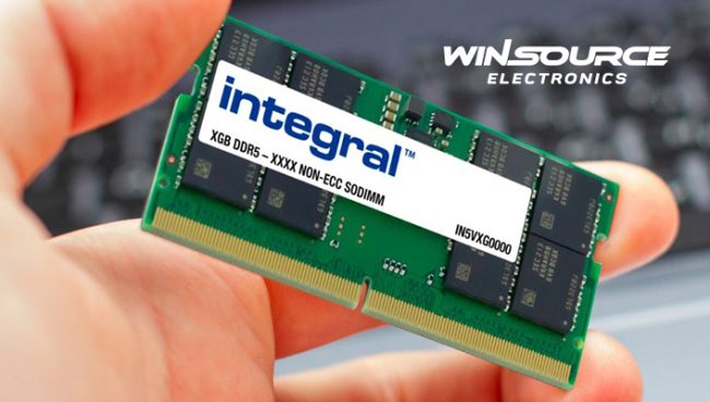
You can find top-notch SDRAMs at WIN SOURCE. They are a reputable electronic components distributor that deals in a multitude of products, including all kinds of RAMs and other electronic-related items.
© 2025 Win Source Electronics. All rights reserved. This content is protected by copyright and may not be reproduced, distributed, transmitted, cached or otherwise used, except with the prior written permission of Win Source Electronics.
COMMENTS