In industrial automation, sensor measurement, and embedded system design, the selection of an analog-to-digital converter (ADC) directly impacts system accuracy, power consumption, and overall cost. Different ADC architectures, such as Delta-Sigma (Δ-Σ) and SAR, each offer distinct performance characteristics suited to specific application scenarios.
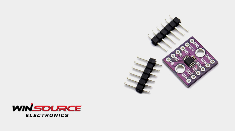
The ADS1118, a highly integrated 16-bit Delta-Sigma ADC from Texas Instruments, features an internal temperature sensor and low-power operation, making it well-suited for certain applications. Represented by the specific model ADS1118IDGST, this device demonstrates strong applicability in industrial measurement and portable equipment.
Key Differences Between ADS1118 and Other ADCs
The ADS1118 adopts a Delta-Sigma (Δ-Σ) architecture and is primarily designed for low-speed, high-precision signal acquisition. Compared with common SAR ADCs or high-speed ADCs, its design emphasizes measurement accuracy and noise immunity.
Resolution and Noise Performance
In low-frequency, high-resolution measurement scenarios, Delta-Sigma ADCs typically offer advantages in effective number of bits (ENOB) and noise suppression. The ADS1118 is capable of reliably handling small signal variations, making it suitable for precision measurements such as temperature, voltage, and pressure.
In contrast, while SAR ADCs provide higher sampling rates, they generally involve trade-offs in low-frequency accuracy and noise performance.
System Integration
A key feature of the ADS1118 is its integrated temperature sensor, which can be used directly for cold junction compensation (CJC) or ambient temperature monitoring, making it particularly suitable for thermocouple-based systems.
Taking ADS1118IDGST as an example, this level of integration helps reduce the number of external components, thereby optimizing system cost and simplifying overall circuit design to a certain extent. This capability is not commonly found in many general-purpose ADCs.
Power Consumption Characteristics
The device supports a single-shot conversion mode, allowing it to enter a low-power state during idle periods, which helps reduce overall system energy consumption. This makes it suitable for battery-powered or remote monitoring applications where power efficiency is an important consideration.
In comparison, high-speed ADCs typically operate continuously, offering less flexibility in power optimization.
Interface and Signal Adaptability
The ADS1118 features a standard SPI interface, providing good compatibility with embedded systems. It also integrates a programmable gain amplifier (PGA), allowing flexible adjustment based on different input signal ranges.
By contrast, some ADCs offer less flexibility in interface options or gain configuration, often requiring additional analog front-end circuitry.
How to Select the Right ADC in Practical Applications
In practical projects, ADC selection is not based on a single parameter comparison, but rather on a comprehensive evaluation of application requirements, including sampling rate, accuracy needs, and system resource constraints. For applications that prioritize real-time performance—such as motor control or high-speed data acquisition—SAR ADCs or high-speed ADCs are typically preferred, as they provide higher sampling rates to meet fast response requirements. In contrast, the ADS1118 is designed for low-speed, high-precision signal acquisition and does not focus on speed. However, it offers advantages in data stability and measurement consistency. Therefore, in applications where speed is not critical but data quality is a priority, its value becomes more evident.
When the design focus shifts toward measurement accuracy, system stability, and overall integration, the advantages of the ADS1118 become more pronounced. Based on the Delta-Sigma (Δ-Σ) architecture, it performs well in low-frequency signal processing and noise suppression, making it suitable for industrial sensing, environmental monitoring, and medical applications. Taking ADS1118IDGST as an example, its integrated temperature sensor and programmable gain amplifier (PGA) help reduce external circuitry, thereby lowering BOM complexity and simplifying the design process—particularly beneficial for space-constrained or fast time-to-market projects. At the same time, its SPI interface provides reliable communication and strong system compatibility; however, in cases where pin resources are limited, I²C-based solutions may be considered as alternatives depending on system architecture. Overall, the key to ADC selection lies in clearly defining application priorities and achieving a balance among performance, power consumption, and system complexity.
In summary, the ADS1118 is not a universal ADC solution for all applications, but rather a device that excels in scenarios requiring low speed, high precision, low power consumption, and high integration. Understanding the differences between ADC architectures enables engineers to make more informed design decisions. For projects evaluating ADS1118IDGST or other ADC solutions, access to a reliable supply chain and professional support is equally important. As an electronic component distributor, Win Source provides high-quality component sourcing and procurement support, helping engineering teams accelerate project development and deployment.
© 2026 Win Source Electronics. All rights reserved. This content is protected by copyright and may not be reproduced, distributed, transmitted, cached or otherwise used, except with the prior written permission of Win Source Electronics.
COMMENTS