In cost-sensitive FPGA designs, device selection should not be based on unit price alone. Engineering teams also need to consider logic resources, I/O count, package size, power budget, development tool support, and supply stability. XC7A100T-1CSG324I belongs to the AMD/Xilinx Artix-7 FPGA family. It is suitable for applications that require a certain level of logic capacity, interface resources, and signal processing capability while keeping system cost and power consumption under control. For industrial control, communication interfaces, data acquisition, embedded signal processing, and medium-complexity vision processing systems, it can serve as a mid-range FPGA option that balances resource scale, package density, and system integration capability.
Evaluating System Resource Fit
The core value of XC7A100T-1CSG324I lies in its relatively balanced resource configuration. The XC7A100T device provides approximately 101,440 logic cells, along with DSP slices and on-chip memory resources. For systems that require parallel logic, interface control, data buffering, and some digital signal processing, this resource combination is generally more flexible than lower-capacity FPGAs and easier to control in terms of overall cost than higher-end devices. In actual design work, engineers should not only check whether the number of logic cells is sufficient. LUTs, flip-flops, block RAM, DSP resources, and I/O resources should also be evaluated together.
FPGA resource consumption usually comes from multiple modules, including state machines, communication interfaces, FIFOs, clock domain handling, DSP operations, memory control, and debugging logic. If the design includes DDR interfaces, LVDS, ADC data input, or multi-channel control logic, a single resource metric is usually not enough to support a complete selection decision. Cost-sensitive designs also need to avoid over-specification. An FPGA with significantly more resources than needed may increase procurement, power supply, PCB, and thermal costs. If the resource margin is too limited, later feature changes or version upgrades may require a new device selection. A more practical approach is to reserve an appropriate design margin based on estimated logic utilization, future feature expansion, and debugging resource requirements.
Package I/O and Board-Level Design Should Be Considered Together
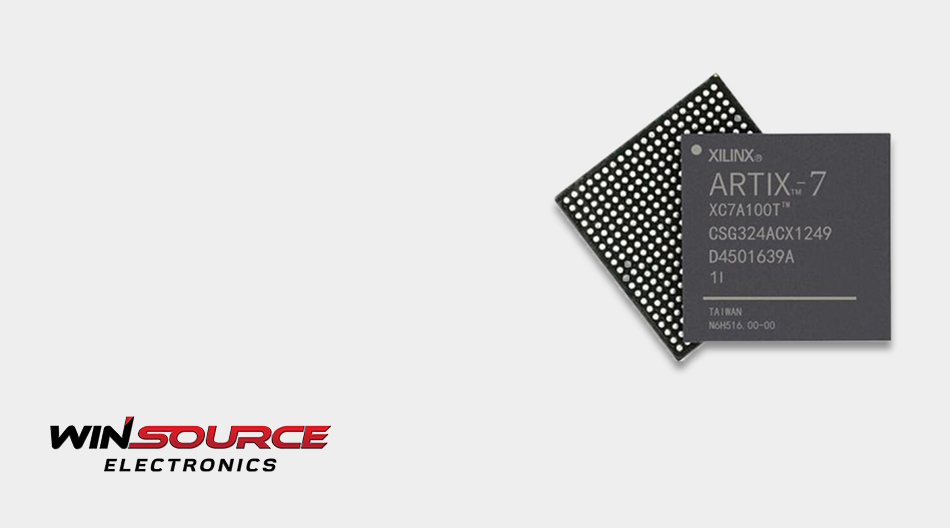
XC7A100T-1CSG324I uses the CSG324 package, which supports relatively high-density connections within limited PCB space. For cost-sensitive systems, package selection can directly affect PCB layer count, routing difficulty, test strategy, and manufacturing cost. The unit price of the FPGA is only one part of the system cost. Board-level implementation cost should also be included in the overall evaluation.
I/O planning must be confirmed early in the selection stage. Engineering teams should not only count the number of functional interfaces. They also need to check the following factors:
- whether the available I/O count can meet current design requirements
- whether the voltage bank arrangement matches different interface voltage levels
- whether interface standards, clock inputs, and configuration pins create any constraint conflicts
- whether debugging interfaces, test points, and spare signals are sufficiently reserved
- whether future expansion interfaces may affect the current pin planning
If the project is sensitive to cost control, preliminary pin planning should be completed before schematic design. This helps determine earlier whether the CSG324 package fits the current system structure. It can also reduce rework caused by pin assignment, signal integrity, or power integrity issues at later stages. For industrial control, communication interfaces, or other equipment with higher stability requirements, package and I/O planning should move forward together with power design, clock architecture, and thermal evaluation.
Power Budget and Application Boundaries Should Be Defined Early
The Artix-7 series is commonly used in cost- and power-sensitive applications, but power evaluation should still not be overlooked. The actual power consumption of an FPGA is affected by logic utilization, clock frequency, I/O switching rate, DSP usage, operating temperature, and power architecture. The same XC7A100T-1CSG324I device may show different power behavior in different systems. Therefore, engineering teams should establish a power budget early in the design stage and evaluate the requirements of the core supply, auxiliary supply, and I/O supplies separately. If the system is deployed in an industrial environment, an enclosed enclosure, or a high-temperature condition, thermal design margin should also be reserved.
From a system selection perspective, XC7A100T-1CSG324I is better suited for FPGA designs with clear resource requirements, controlled power budgets, and moderate interface counts. If the project requires larger logic capacity, higher bandwidth, or more complex high-speed interfaces, the broader device family should be reviewed. If the project is mainly used for simple glue logic or low-speed control, this device may be over-specified.
Overall, XC7A100T-1CSG324I is suitable for designs that need to balance cost, power consumption, and mid-range FPGA resource requirements. Proper selection should not depend on whether a single device parameter appears sufficient. Instead, logic resources, I/O planning, package implementation, power budget, and application boundaries should be evaluated within the same system framework. For engineering teams working on BOM management, alternative part confirmation, or long-term supply planning, WIN SOURCE can support part information checks, inventory matching, and procurement assistance based on the specific model and project requirements, helping make the selection process more controlled and reliable.
© 2026 Win Source Electronics. All rights reserved. This content is protected by copyright and may not be reproduced, distributed, transmitted, cached or otherwise used, except with the prior written permission of Win Source Electronics.
COMMENTS