
*Image from the internet; all rights belong to the original author, for reference only.
Intel Brings High-NA EUV into Panther Lake Production
Quick Take
- Intel is using ASML’s High-NA EUV technology in high-volume manufacturing for specific layers of select Panther Lake processors.
- The products are built on Intel 18A, with the High-NA process qualified alongside ASML’s established NXE platform.
- The milestone demonstrates production readiness, but it does not mean every Panther Lake layer or processor uses High-NA EUV.
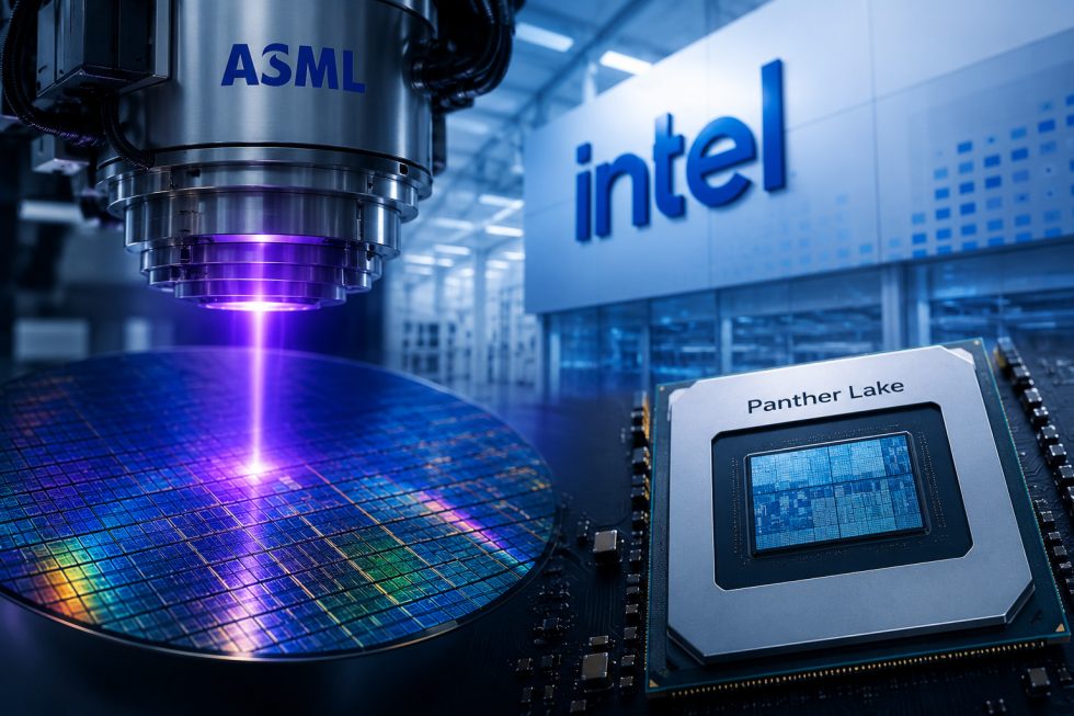
On July 15, 2026, ASML confirmed that Intel Foundry had introduced High-NA EUV into high-volume logic manufacturing. The technology is being used on specific Intel 18A layers for a subset of Intel Core Ultra Series 3 processors, code-named Panther Lake. According to ASML, products are already shipping to customers at yields matched to its established NXE platform. The announcement moves High-NA EUV beyond laboratory development and into commercial production, while also showing that adoption will initially be selective rather than immediate across every chip layer.
Q1. What exactly did ASML and Intel announce?
Intel Foundry is using ASML’s EXE High-NA EUV technology to manufacture specific layers of select Panther Lake processors. These processors belong to the Intel Core Ultra Series 3 family and are built on the Intel 18A process.
The relevant layers have been dual-qualified on High-NA EUV and ASML’s existing NXE platform at Intel’s Oregon facility. This gives Intel manufacturing flexibility while providing production data on system setup, uptime, yield and process implementation.
ASML also confirmed that the processors are shipping to customers and described Intel as the first company to ship a high-volume logic product using High-NA EUV. However, the announcement applies only to a subset of processors and selected layers—not the complete Panther Lake product line or every Intel 18A manufacturing step.
Q2. What is High-NA EUV, and how is it different from current EUV systems?
High-NA EUV is the next generation of extreme ultraviolet lithography used to print small circuit patterns onto silicon wafers. “NA” means numerical aperture, a measure related to an optical system’s ability to collect and focus light.
ASML’s established NXE systems have a numerical aperture of 0.33, while the newer EXE platform increases it to 0.55. Both use EUV light with a wavelength of 13.5 nanometers, but the higher numerical aperture improves imaging resolution.
According to ASML, its EXE systems provide 8-nanometer resolution, compared with 13 nanometers for NXE systems. The improved resolution can allow some features to be printed with a single exposure instead of more complex multiple-patterning processes. In practice, this may reduce the number of manufacturing steps for suitable layers, although the benefits depend on the chip design and process configuration.
Q3. Why is the Panther Lake milestone important?
The key change is that High-NA EUV has moved into a real high-volume production environment.
Installing a lithography system or producing experimental wafers does not prove that the technology is ready for commercial manufacturing. A production process must also demonstrate acceptable yield, overlay accuracy, output, stability and integration with other wafer-fabrication steps.
Intel and ASML began integrating their first commercial High-NA EUV system in Oregon in 2024. Intel later installed and completed acceptance testing for the second-generation TWINSCAN EXE:5200B. The latest announcement shows that the technology is now being used for customer products rather than only process development.
The dual qualification with NXE is also significant because it gives Intel an existing production option while it continues learning how to use High-NA EUV more broadly.
Q4. Does every Panther Lake processor now use High-NA EUV?
No. ASML carefully states that High-NA EUV is being used for specific Intel 18A layers in a subset of Intel Core Ultra Series 3 processors.
A modern processor requires many patterned layers, and chipmakers may use different lithography techniques depending on the dimensions, complexity and economics of each layer. High-NA EUV is therefore one part of the manufacturing flow, not a replacement for every existing lithography system.
This distinction matters when evaluating the maturity of the technology. The announcement proves that High-NA EUV can be integrated into high-volume logic production, but broader adoption will depend on manufacturing results, process costs and the requirements of future nodes.
ASML says Intel retains the flexibility to introduce the technology into future processes according to customer and product needs.
Q5. Which products and component markets could eventually benefit?
High-NA EUV is designed to support advanced logic and leading-edge memory manufacturing. Potential applications include future CPUs, AI accelerators, data-center processors and high-performance mobile chips that require greater transistor density and improved energy efficiency.
ASML also positions the EXE:5200B for sub-2nm logic processes and leading-edge DRAM. That makes the technology relevant not only to processors but also to future memory ICs used in AI servers, high-performance computing and other data-intensive systems.
For complete electronic systems, progress in advanced processors can influence demand for adjacent components such as server memory, power management ICs, voltage regulators and high-speed interconnects. However, this manufacturing milestone does not establish an immediate shortage or price increase in those categories. Their supply conditions must still be evaluated independently.
Q6. What should the industry watch next?
The next question is how quickly High-NA EUV expands from selected production layers to broader use in future logic and memory nodes.
Important signals will include additional customer qualifications, manufacturing throughput, uptime, defect control and whether chipmakers can reduce multiple-patterning steps without creating new cost or process challenges. Wider deployment of the EXE:5200B will also provide more evidence of production maturity.
For Intel, the industry should watch whether High-NA EUV is incorporated more extensively into later Intel 18A products or future nodes. For ASML, progress will be measured by customer acceptance and the transition from early production use to repeatable deployment across multiple fabs.
The July announcement confirms an important production milestone, but broader industry adoption will develop over several product and process cycles.
Conclusion
Intel’s use of High-NA EUV for selected Panther Lake layers is an important step from technology development to commercial logic production. It demonstrates that ASML’s EXE platform can operate within a high-volume manufacturing flow while remaining complementary to existing NXE systems. The next indicators will be broader customer qualification, manufacturing performance and adoption in future logic and DRAM nodes—not simply the number of systems installed.
© 2026 Win Source Electronics. All rights reserved. This content is protected by copyright and may not be reproduced, distributed, transmitted, cached or otherwise used, except with the prior written permission of Win Source Electronics.

COMMENTS