
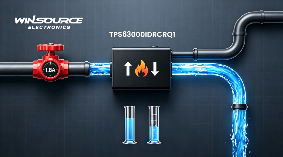
TPS63000IDRCRQ1 features 1.8 A internal power switches, but this specification should not be directly interpreted as the continuous output current capability under all operating conditions. The available load current varies depending on input voltage, output voltage setting, buck-boost operating mode, conversion efficiency, thermal conditions, and external component selection. This article explains how to properly evaluate the actual output capability of TPS63000IDRCRQ1 by analyzing switch current limits, current behavior in buck and boost modes, and worst-case system validation.
1. The 1.8 A Rating Refers to Internal Switch Current
TPS63000IDRCRQ1 uses a four-switch synchronous buck-boost topology, allowing a single inductor to support buck operation, boost operation, and automatic transition between the two modes. The 1.8 A specification in the datasheet refers to the typical average current limit of the internal power switches. It indicates the current capability of the power stage but does not represent the continuous load current that can always be delivered at the output.
In buck mode, when the input voltage is higher than the output voltage, the average inductor current is relatively close to the output current. However, factors such as current limit tolerance, inductor ripple current, conversion losses, and thermal rise must also be considered.
According to TI’s typical application data, when configured for a 3.3 V output with a 3.6 V to 5.5 V input voltage, TPS63000IDRCRQ1 can support up to approximately 1.2 A output current. Even under this relatively favorable buck operating condition, the available output current remains below the 1.8 A internal switch current rating.
2. Why Output Current Further Decreases in Boost Mode
When the input voltage falls below the configured output voltage, the converter operates in boost mode. In this condition, output power is supplied from a lower input voltage, requiring higher current on the input and inductor sides.
Based on power conversion principles, the output current is mainly limited by input voltage, available input current, conversion efficiency, and output voltage. As the input voltage decreases, a higher inductor current is required to maintain the same output power, making the system more likely to approach the internal switch current limit.
For a 3.3 V output configuration, TI’s specifications indicate that when the input voltage is above 2.4 V in boost mode, the device can provide approximately 800 mA maximum output current. As the input voltage continues to decrease, the available output current will be further reduced.
In single-cell battery applications, the converter may operate through different regions as the battery voltage changes during discharge, including buck mode, buck-boost transition, and boost mode. Therefore, load capability should not be evaluated only based on the nominal battery voltage.
The buck-boost transition region also requires careful consideration. When the input voltage approaches the output voltage, the device automatically adjusts the operation of its four power switches to maintain a stable output. Under these conditions, current stress is also affected by the inductor value, inductor saturation current, output capacitance, PCB parasitic effects, and load transient behavior.
3. System-Level Selection Should Be Based on Worst-Case Conditions
When designing with the TPS63000IDRCRQ1, its output capability should be evaluated at the minimum input voltage, maximum load, target output voltage, and highest expected ambient temperature. The 1.8 A switch rating should not be treated as the available design output current. Key system-level checks include:
Maintaining the required output voltage at the minimum battery operating voltage;
- Ensuring that peak load demand and startup inrush current do not drive the inductor current close to the device current limit;
- Providing sufficient saturation-current margin in the selected inductor;
- Verifying that the effective input and output capacitance remains adequate under DC-bias conditions;
- Providing sufficient thermal-pad design and PCB copper area for the 3 mm × 3 mm VSON package;
- Confirming that Power-Save mode or fixed-frequency operation meets the system requirements for efficiency, output ripple, and EMI.
Prototype validation should extend beyond steady-state output current measurements to cover minimum input voltage, load transients, cold startup, high-temperature operation, and increased battery impedance. If output voltage drops, ripple increases, or device temperature rises significantly under these conditions, input voltage, inductor current, and output waveforms should be evaluated together to determine whether the limitation originates from insufficient input power, power-stage current stress, or PCB layout.
The 1.8 A specification of TPS63000IDRCRQ1 represents the typical current limit of its internal switches rather than a fixed output current rating. The actual output capability depends on the buck-boost operating condition, input-to-output voltage relationship, efficiency, thermal performance, and external component selection. For projects requiring long-term supply stability and batch consistency, WIN SOURCE can support component sourcing, batch information verification, and supply coordination. However, the actual output capability of TPS63000IDRCRQ1 in the target application should always be confirmed through worst-case system testing.
© 2026 Win Source Electronics. All rights reserved. This content is protected by copyright and may not be reproduced, distributed, transmitted, cached or otherwise used, except with the prior written permission of Win Source Electronics.

COMMENTS