Overview
The FDC6312P is a dual P-channel power MOSFET from Onsemi , employing PowerTrench® trench MOSFET technology optimized for low on-resistance and low gate charge. This device supports a drain-source voltage of −20V and a maximum continuous drain current of −2.3A , while maintaining low on-resistance at lower gate drive voltages, making it particularly suitable for low-voltage power management, load switching, and power path control in portable electronic devices.
The FDC6312P integrates two P-channel MOSFETs in a compact SuperSOT™-6 / TSOT-23 6-pin package, providing dual-channel power control within limited PCB space. The device operates under various gate drive conditions, including VGS = −1.8V, −2.5V, and −4.5V , making it suitable for applications directly driven by low-voltage MCUs, logic controllers, or power management circuitry.
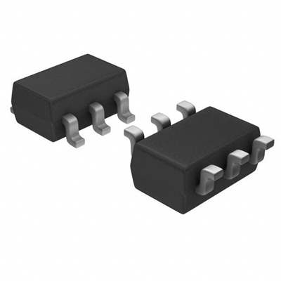
Core parameters
| Parameter | Value |
| Product Type | Dual P-channel power MOSFET |
| Manufacturer | onsemi |
| Number of MOSFETs | 2 P-Channels |
| Drain-source voltage (VDSS) | -20V |
| Continuous drain current (ID) | -2.3A |
| Pulse drain current | -7A |
| RDS(on) | Maximum 115mΩ @ VGS = −4.5V |
| RDS(on) | Maximum 155mΩ @ VGS = −2.5V |
| RDS(on) | Maximum 225mΩ @ VGS = −1.8V |
| Gate threshold voltage | -0.4V to -1.5V |
| Maximum gate-source voltage | ±8V |
| Total gate charge | Maximum 7nC |
| Junction temperature range | -55°C to +150°C |
| Packaging | SuperSOT™-6/TSOT-23 6-Lead |
| Installation method | Surface Mount |
| Environmental standards | Pb-Free / RoHS |
The above main parameters are based on the Onsemi official datasheet.
Features
Dual P-channel structure improves power control integration
The FDC6312P integrates two P-channel MOSFETs in a single device, enabling applications such as dual-load control, power path management, or high-side switching circuits. Compared to solutions using two separate MOSFETs, this helps reduce PCB footprint and the number of external connections.
Low on-resistance reduces power loss
The device is manufactured using Onsemi PowerTrench® technology and has a maximum RDS(on) of 115mΩ at VGS = −4.5V ; even at a low gate drive condition of VGS = −1.8V , the maximum RDS(on) remains at 225mΩ. This characteristic allows it to adapt to different logic voltage systems.
Low voltage gate drive capability
The FDC6312P is a 1.8V specified MOSFET , and its on-resistance can be tested at a gate-source voltage of −1.8V, making it suitable for modern low-voltage digital control systems. For power switching circuits driven by low-voltage MCUs, processors, or logic controllers, it reduces the need for additional gate drive stages.
Low gate charge improves switching performance
The device has a maximum total gate charge of 7nC, with a typical value of approximately 4.4nC. This reduces the gate drive burden while maintaining low on-resistance, which is beneficial for improving dynamic response in load switching and power management applications.
Compact SuperSOT™-6 package
The FDC6312P is packaged in a 6-pin SuperSOT™-6/TSOT-23 package, which offers a smaller PCB footprint and lower package height compared to the standard SO-8 package, making it suitable for portable devices and high-density power supply designs. Onsemi’s official documentation states that this package size reduces the footprint by approximately 72% compared to the standard SO-8.
Typical application scenarios
Power Management
The FDC6312P can be used for low-voltage DC power path control, load switching, and power rail switching, achieving load on/off control through the high-side switching structure of a P-channel MOSFET.
load switch
The dual-channel structure is suitable for circuits that require two independent load controls, such as peripheral module power supply, interface power management, and local power control of embedded systems.
Portable electronic devices
Its low on-resistance, small package size, and low gate drive requirements make it suitable for mobile devices, portable instruments, and battery-powered equipment.
Embedded systems
It can be used with GPIO/logic control signals of MCU, processor or FPGA to realize the power start/stop and power path management of peripheral devices.
Battery-powered system
The high-side switching structure of P-channel MOSFETs can be used for battery load management, enabling a simpler power control scheme in low-voltage systems.
Comparative Advantage Analysis
| Performance indicators | FDC6312P | Standard single MOSFET |
| Number of MOSFETs | Dual Channel | single channel |
| Channel type | P-Channel | Depending on the model |
| Maximum VDSS | -20V | Depending on the model |
| Continuous drain current | -2.3A | Depending on the model |
| low voltage drive | Supports up to 1.8V specifications. | Partial support |
| RDS(on) | As low as 115mΩ Max | Depending on the model |
| Packaging | SuperSOT™-6 | Standard SOT-23, etc. |
| PCB integration | high | generally |
The main advantages of the FDC6312P are its dual P-channel integration, low-voltage gate drive, low RDS(on), and small package . For space-constrained embedded systems requiring multiple power supply control, it can reduce the number of discrete components and improve PCB integration .
Manufacturer Profile: onsemi
OnSemi is a leading global supplier of power semiconductors and smart sensing solutions, with products including MOSFETs, IGBTs, SiC power devices, power management ICs, sensors, and interface devices.
The FDC6312P belongs to the onsemi PowerTrench® MOSFET product family, which optimizes on-resistance and switching performance through trench technology and is widely used in power management, load switching and low-voltage power control applications.
Why choose FDC6312P?
● Dual P-channel MOSFET integration, suitable for dual power supply control
● −20V drain-source withstand voltage, meeting various low-voltage power supply applications
● Maximum −2.3A continuous drain current
● Supports 1.8V-level low-voltage gate drive
● RDS(on) as low as 115mΩ Max @ VGS = −4.5V
● Maximum total gate charge of only 7nC, facilitating fast switching
● SuperSOT™-6 small package, suitable for high-density PCBs
● −55°C to +150°C wide junction temperature range, meeting harsh operating environments
Frequently Asked Questions (FAQ)
Q1: Is the FDC6312P a single MOSFET or a dual MOSFET?
The FDC6312P is a dual P-channel MOSFET that integrates two P-channel devices in a single package, making it suitable for dual- load control or power management circuits that require two MOSFETs.
Q2: Is the FDC6312P suitable for a 1.8V logic system?
Suitable. This model is a 1.8V specified P-channel MOSFET , and the datasheet provides the RDS(on) specification under VGS = −1.8V conditions, with a maximum value of 225mΩ. Therefore, it has good compatibility in low-voltage logic control systems.
For more details and to explore our inventory, please visit the following link:
Product Details: Win Source – FDC6312P
Price: Win Source – FDC6312P
©2026 Win Source Electronics. All rights reserved. This content is protected by copyright and may not be reproduced, distributed, transmitted, cached or otherwise used, except with the prior written permission of Win Source Electronics.