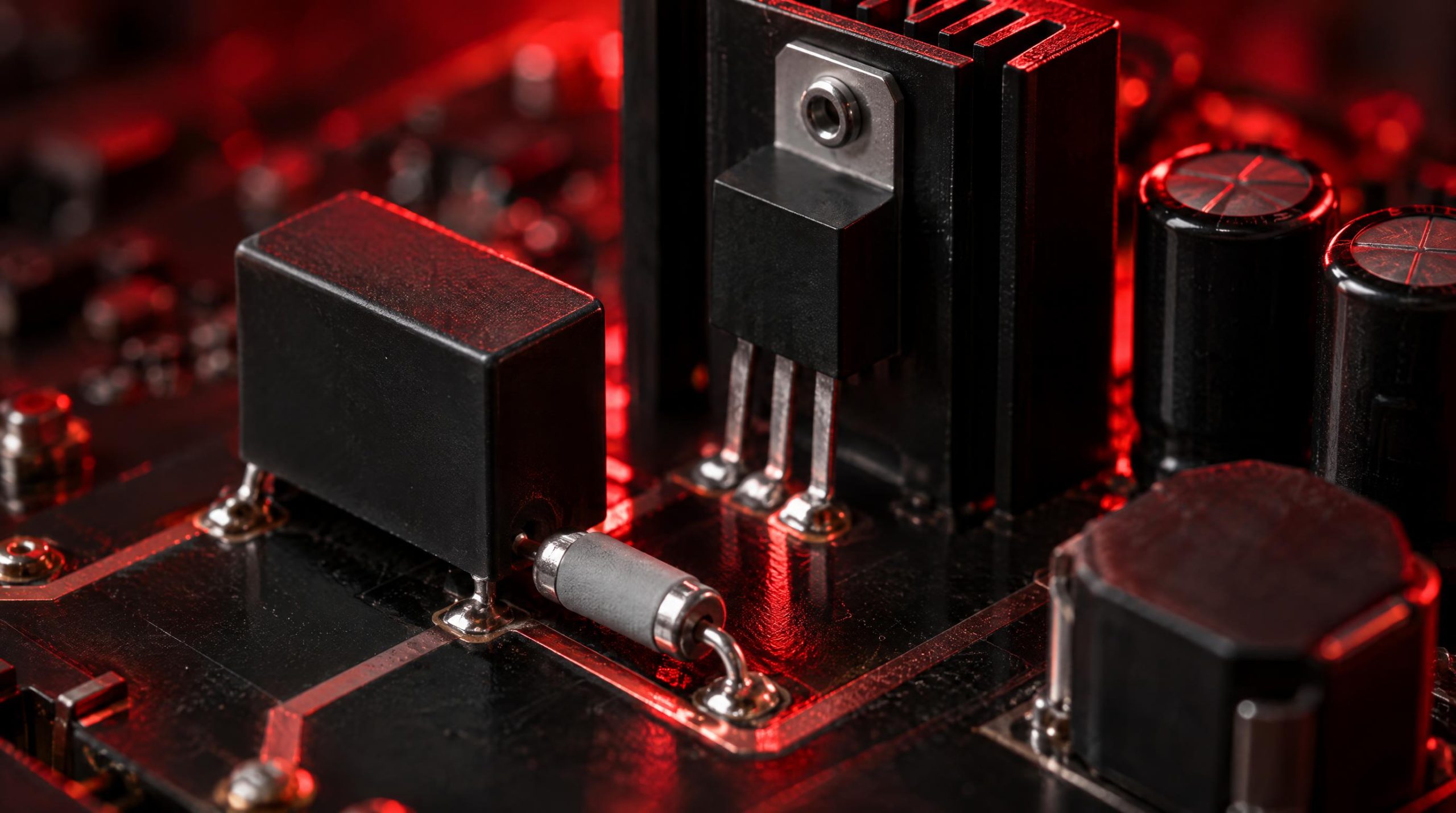
Every time a power switch opens, the energy stored in the circuit’s parasitic inductance has to go somewhere. In a well-designed system, a snubber circuit absorbs that energy before it becomes a voltage spike sharp enough to destroy a MOSFET, IGBT, or diode. In a poorly designed one, the spike finds the weakest component instead.
Snubber circuits have been a staple of power electronics since the earliest thyristor converters, and they remain just as relevant today — arguably more so, because modern wide-bandgap devices like SiC MOSFETs switch so fast that even a few nanohenries of stray inductance can generate dangerous transients. This article explains the physics behind switching transients, walks through the main snubber topologies and their trade-offs, and offers practical guidance on component selection and PCB layout. Whether you are designing a flyback converter, a motor drive inverter, or an industrial power supply, the principles apply across the board.
How to tame voltage spikes in switching designs — topologies, component selection, and PCB layout best practices.
|
⚡ MOSFETs & IGBTs
|
4 Passive Topologies
|
PCB Layout Rules
|
|
300V
Spike from 100nH @ 30A
|
<10ns
SiC/GaN switch time
|
4×
Min snubber C vs Coss
|
|
Why Voltage Spikes Happen
|
|
⚡
|
V = L × dI/dtInductance opposes instantaneous current change. When a switch opens, any stray loop inductance (PCB traces, leads, bus bars) generates voltage proportional to the switch speed. Even 50 nH of stray inductance with sub-10 ns transitions can exceed 100 V of overshoot — pushing devices past breakdown voltage. |
Parasitic inductance + switch output capacitance (Coss) form an LC tank circuit that rings into the hundreds of MHz — generating sustained EMI that can violate CISPR 32 limits without external damping.
|
4 Functions a Snubber Provides
|
|
Spike Suppression
Absorbs energy before it becomes a destructive voltage transient across the switch |
SOA Compliance
Shapes switching trajectory to stay within the device’s Safe Operating Area limits |
|
EMI Reduction
Damps LC resonance to reduce radiated & conducted EMI for regulatory compliance |
⚙️
Loss Reduction
Controls dV/dt at turn-on to reduce overlap of high V and high I across the switch |
|
Snubber Topology Comparison
|
Choose based on your frequency, efficiency, and complexity requirements
C Snubber
|
RC Snubber
|
Discharge RCD
|
Non-Discharge RCD
|
|
Component Selection Rules
|
|
Critical Damping Condition
Rs = √(L/C) Measure ringing freq on oscilloscope post turn-off
Back-calculate parasitic L and C from measurement
RC time constant = 1/5 to 1/10 of switching period
Empirical start: ~150 Ω + 1 nF for mid-power boost
|
✅ Capacitor Rules
▸ Film caps only — polyester or polypropylene (low ESL, pulse-rated)
▸ Voltage rating 1.5–2× max operating voltage
✗ Never use electrolytic — high ESL, poor HF performance
✅ Resistor Rules
▸ Carbon composition or metal film for low self-inductance
✗ Wire-wound only if specifically rated non-inductive
✅ Diode Rules
▸ Fast or ultra-fast recovery diodes — standard practice
✗ Slow recovery diodes introduce their own current spike
|
|
PCB Layout: The Critical Factor
|
⚠️ A correctly calculated snubber can still fail if PCB layout adds parasitic inductance between the snubber and the switch.
|
Mount as Close as Possible
Every mm of trace between snubber and switch adds loop inductance in series with what you’re cancelling |
↔️
Short & Wide Traces
Form the smallest possible current loop with low-inductance traces connecting snubber to device terminals |
|
IGBT Direct-Mount
Use direct-mount capacitor assemblies connecting straight to collector/emitter terminals on IGBT modules |
Laminated Bus Bars
Reduce total parasitic inductance in high-current designs — allowing smaller, lower-loss snubber components |
|
Application-Specific Guidance
|
|
Flyback Converters
RCD clamp snubber across primary switch. Set clamp voltage to 2–2.5× reflected output voltage. Leakage inductance is the main spike source. |
Motor Drive Inverters
Non-discharge RCD preferred for continuous duty. Bus-level + per-device snubbers needed with long motor cables due to reflected voltage waves. |
|
SiC & GaN Converters
Layout optimization first, snubber second. Good layout may need only a small C snubber. Poor layout forces large dissipative networks that erode efficiency gains. |
|
5 Key Takeaways
|
|
1
|
V = L × dI/dt is the root cause — stray loop inductance plus fast switching speed generates every dangerous transient in your circuit. |
|
2
|
Match topology to application — RC for general use, discharge RCD for better clamping, non-discharge RCD for high-frequency efficiency. |
|
3
|
Film capacitors only — polyester or polypropylene, rated 1.5–2× max voltage, sized at minimum 4× switch Coss. |
|
4
|
PCB layout is not optional — mount snubber components directly adjacent to the switch with short, wide, minimum-loop-area traces. |
|
5
|
Always verify on the bench — calculated values are starting points; real PCB parasitics require oscilloscope-guided iterative tuning. |
|
Need Snubber Components?
Film caps · Fast-recovery diodes · TVS & circuit protection — current-production and hard-to-find parts.
|
Submit an RFQ → |
| WIN SOURCE — Global independent distributor of electronic components | win-source.net |
Why Voltage Spikes Happen in Switching Circuits
Why Voltage Spikes Happen in Switching Circuitsge spikes in switching circuits is straightforward: inductance opposes any instantaneous change in current, and switching devices change current very quickly. When a MOSFET or IGBT turns off, the current that was flowing through the switch must redirect almost instantaneously. Any inductance in the current loop — the PCB traces, the component leads, the bus bars — responds by generating a voltage proportional to the rate of change: V = L × dI/dt. A 30 A load current switched off in 10 ns through just 100 nH of parasitic inductance produces a 300 V spike on top of the bus voltage. With modern wide-bandgap devices achieving sub-10 ns transition times, even 50 nH of stray inductance can generate transients exceeding 100 V — enough to push a device well past its rated breakdown voltage.
The situation is compounded by the resonant interaction between parasitic inductance and the switch’s output capacitance (Coss). After the initial spike, these two elements form an LC tank that rings at a frequency which can reach into the hundreds of megahertz. The oscillation decays slowly without external damping, producing sustained voltage overshoot and radiated EMI that can violate regulatory limits such as CISPR 32. The challenge for designers is to damp this ring quickly without introducing excessive losses or slowing the switching transition so much that efficiency suffers.
What a Snubber Circuit Actually Does
What a Snubber Circuit Actually Does network — typically passive, occasionally active — placed across a switching device or a diode to control transient voltage and current behavior. The word comes from the mechanical engineering term for a device that absorbs shock, and the analogy is apt: a snubber absorbs the electromagnetic energy that would otherwise appear as a destructive spike. Depending on the topology, a snubber may dissipate that energy as heat, redirect it back into the supply, or temporarily store it and release it at a less harmful moment in the switching cycle.
Snubbers serve several overlapping purposes. They protect semiconductor devices from exceeding their voltage ratings. They reduce dV/dt and dI/dt stress, keeping the switching trajectory within the device’s safe operating area (SOA). They damp the high-frequency ringing that causes EMI. And in some configurations, they actively reduce switching losses by shaping the turn-on and turn-off waveforms. No single snubber topology does all of these things optimally, which is why understanding the trade-offs between types matters.
Snubber Circuit Types and When to Use Each
Snubber Circuit Types and When to Use Eachthe vast majority of real-world snubber designs. Each adds components and complexity relative to the last, and each offers a different balance between cost, efficiency, and protection effectiveness.
C Snubber
The simplest snubbe>C Snubberapacitor placed directly across the switch. The capacitor limits the rate of voltage rise (dV/dt) during turn-off by providing a low-impedance path that slows the voltage transition. It also absorbs the energy stored in the stray inductance, preventing it from appearing as a spike. The C snubber is cheap and easy to implement, but it has a significant drawback: the capacitor discharges entirely through the switch at turn-on, creating an additional current pulse that increases turn-on losses. For this reason, the C snubber alone is more common in low-frequency or single-shot applications than in high-frequency converters.
RC Snubber
Adding a series re>RC Snubberpacitor gives the RC snubber — the most widely used configuration in power electronics. The resistor serves two functions: it limits the peak current when the capacitor discharges at turn-on, and it damps the LC resonance by adding resistive loss to the tank circuit. The capacitor absorbs the voltage spike and reduces dV/dt across the switch, while the resistor dissipates the stored energy as heat. The RC snubber is straightforward to design, widely available as a pre-assembled module, and effective across a broad range of switching frequencies. Its main limitation is continuous power dissipation — the resistor burns energy on every switching cycle, which reduces converter efficiency, particularly at higher switching frequencies where the capacitor charges and discharges more often per second.
Discharge RCD Snubber
The dischar>Discharge RCD Snubberde in parallel with the resistor. During the turn-off transient, the diode bypasses the resistor and allows the capacitor to charge quickly through a very low impedance path, which maximizes surge absorption. When the switch turns back on, the capacitor discharges through the resistor (the diode blocks reverse current), which limits the turn-on current surge. This configuration provides better spike suppression than a plain RC snubber for the same component values. However, designers must pay careful attention to the diode’s reverse recovery characteristics — a slow diode can introduce its own current spike during recovery, partially defeating the purpose of the circuit. Fast or ultra-fast recovery diodes are standard practice here.
Non-Discharge RCD Snubber
The non-d>Non-Discharge RCD Snubber uses a different topology in which the resistor-diode combination is arranged so that the snubber capacitor does not fully discharge on every switching cycle. Instead, it only dissipates the incremental energy absorbed during each overvoltage event. Because the capacitor voltage stabilizes at a clamping level rather than resetting to zero each cycle, significantly less energy is wasted — making this configuration the most efficient of the four passive types and particularly well suited to high-frequency operation. The trade-off is that the clamping voltage must be chosen carefully; set it too high and the spike suppression is inadequate, set it too low and the resistor dissipation increases.
Active and Lossless Snubbers
Beyond t>Active and Lossless Snubberstive snubbers use additional switches and reactive components to recover the snubber energy rather than dissipating it. Lossless LC snubbers, for example, return the energy captured from stray inductance back to the supply rail or load through a resonant path. Active snubbers are common in high-power applications such as large industrial inverters or EV traction drives, where even small percentage efficiency gains translate to significant energy savings at scale. The added control complexity and component count make them less practical for low- to mid-power designs where a well-optimized passive RCD snubber is usually sufficient.
Four Protection Functions Snubbers Provide
Four Protection Functions Snubbers Providet helps clarify why they are placed where they are and how to evaluate whether a given design is working.
Voltage spike and ringing suppression. This is the primary function. Without a snubber, the drain-source voltage of a switching MOSFET can spike far beyond the bus voltage during turn-off — measurements on unprotected circuits routinely show oscillations that push devices into or beyond their breakdown regions. The snubber capacitor provides an alternative current path during the switching transition, absorbing the energy that would otherwise create that spike and damping the subsequent ringing.
Safe Operating Area (SOA) compliance. Power semiconductor datasheets define an SOA — a bounded region in the voltage-current plane within which the device can operate without damage. Hard switching without snubbers creates a switching trajectory that traces a wide rectangular path through the SOA, simultaneously imposing high voltage and high current during the transition. Snubbers shape that trajectory into a narrower path by staggering the voltage and current peaks in time, keeping the device safely inside its SOA limits. This is particularly important during power-up transients and fault conditions.
Resonance suppression and EMI reduction. The LC resonance formed by circuit parasitic elements generates high-frequency ringing that radiates as EMI and can couple into control circuitry, gate drives, and signal lines. A well-designed snubber increases the resistive damping in the resonant circuit, compressing the impedance peak and smoothing out abrupt phase transitions. The result is a flatter impedance profile across frequency, which directly reduces radiated and conducted EMI — a prerequisite for passing regulatory certification in most markets.
Switching loss reduction. This may seem counterintuitive given that snubbers dissipate energy themselves, but by controlling dV/dt during turn-on, a snubber reduces the overlap period during which both voltage and current are simultaneously high across the switch. In soft-switching topologies such as zero-voltage switching (ZVS) converters, optimized snubbers combined with gate resistance tuning can reduce turn-off energy losses significantly compared to hard-switched circuits with no snubber network.
Practical Design and Component Selection Guidance
Practical Design and Component Selection Guidance to measure the natural ringing frequency at the switch node using an oscilloscope after turn-off. From this measurement, the parasitic LC values of the circuit can be back-calculated, which in turn gives the target impedance the snubber resistor must match to achieve critical damping. The critical damping condition is approximately R_s = √(L/C), and the snubber capacitor should be chosen larger than the resonant capacitance — typically at least four times the switch output capacitance (Coss) — to shift the resonant frequency downward and reduce spike amplitude. Starting values of around 150 Ω and 1 nF are commonly cited as empirical defaults for moderate-power boost converters, but these should always be verified on the bench.
Component type matters as much as value. Snubber capacitors are exposed to high peak currents, high dV/dt, and repetitive charge-discharge cycles. Film capacitors (polyester or polypropylene) are the standard choice because they handle pulse stress well and have low equivalent series inductance (ESL). Electrolytic capacitors are not suitable for snubber use — their high ESL and poor high-frequency performance make them ineffective in this role. Voltage derating is also critical: standard practice is to select a capacitor rated for at least 1.5 to 2 times the maximum voltage it will see in service, accounting for the overshoot the capacitor itself experiences during snubbing. For resistors, carbon composition or metal film types are preferred because of their low self-inductance; wire-wound resistors should be avoided unless they are specifically rated as non-inductive, as any series inductance partially defeats the snubber’s purpose.
The RC time constant of the snubber (τ = RC) should be shorter than the switching period but long enough to damp high-frequency oscillations. A useful rule of thumb is that the time constant should be roughly one-fifth to one-tenth of the switching period. Iterative bench tuning with an oscilloscope is almost always required to find the optimum point between adequate spike suppression and acceptable power dissipation — calculated starting values get you close, but parasitics in real PCBs rarely match the idealized model exactly.
PCB Layout: The Factor Most Designers Underestimate
Eve>PCB Layout: The Factor Most Designers Underestimatehe PCB layout introduces additional parasitic inductance between the snubber components and the switching device. Every millimeter of trace between the snubber capacitor and the switch terminals adds loop inductance — and that added inductance is in series with the parasitic inductance the snubber is trying to cancel. The practical result is higher-than-expected voltage spikes and reduced damping effectiveness. The single most important layout rule is to mount the snubber components as close as physically possible to the switching device, with short, wide, low-inductance traces forming the smallest possible current loop.
For IGBT modules in high-power inverters, direct-mount snubber capacitor assemblies that connect straight to the module’s collector and emitter terminals are available from several component manufacturers, and these should be strongly preferred over snubber components mounted on a distant PCB location. In bridge and half-bridge topologies, small low-ESL DC bus capacitors placed immediately adjacent to the switch devices serve a complementary function by reducing the bus inductance seen by the snubber, making the snubber more effective per unit of capacitance. Using laminated bus bars in high-current designs is another effective way to reduce the total parasitic inductance that the snubber has to manage, which in turn allows smaller, lower-loss snubber components.
Application-Specific Considerations
Flyback conve>Application-Specific Considerations applications requiring snubbers. When the primary-side MOSFET turns off, the leakage inductance of the transformer resonates with the MOSFET’s output capacitance to produce a high-voltage spike on the drain. An RCD clamp snubber across the primary switch is the standard solution, with the snubber capacitor voltage set to approximately 2 to 2.5 times the reflected output voltage. Getting this ratio right is important: setting the clamp too low wastes too much energy in the resistor, while setting it too high allows excessive voltage stress on the MOSFET.
Motor drive inverters present a different challenge. In three-phase bridge topologies, each switching event in one leg interacts with the bus inductance shared by all six switches. Bus-level snubbers placed across the DC link capacitor help, but individual device snubbers are often needed as well when long motor cables are involved, since cable capacitance can cause reflected voltage waves that arrive back at the inverter output terminals with significant amplitude. The non-discharge RCD topology is generally preferred here because of its lower average power dissipation across the high switching frequency and continuous duty cycle of a motor drive.
SiC and GaN switching converters deserve special mention because their very fast switching transitions — the feature that makes them efficient — also make them the most sensitive to stray inductance. The snubber design process for these devices demands particularly careful PCB layout optimization, and in many cases the primary solution is to minimize parasitic inductance through layout before sizing a snubber, rather than compensating for a poor layout with a larger snubber. A well-laid-out SiC design may need only a small C snubber or no snubber at all; a poorly laid-out one will require a larger dissipative network that erodes the efficiency advantage the device was chosen to provide.
Sourcing Snubber Components
Snubber designs typically call fo>Sourcing Snubber Componentsts — film capacitors, resistors, and fast-recovery diodes — but sourcing the right specifications in production quantities is not always straightforward. Film capacitors with the right voltage rating, capacitance, and low ESL for a specific snubber application may be available from only a handful of manufacturers, and certain high-voltage, high-pulse-current ratings can be difficult to locate outside of specialty distributors. Fast-recovery diodes rated for the peak current and reverse voltage of a given snubber topology also have a range of specifications that narrows the field of suitable parts considerably.
For production designers, having a reliable supply of film capacitors suited to snubber use and fast-recovery diodes is a routine procurement consideration that can turn into a shortage problem if a key component goes end-of-life or faces supply constraints — especially for long-production-run industrial or automotive designs. WIN SOURCE, a global independent distributor of electronic components, stocks these parts across current-production and hard-to-find part numbers and supports shortage sourcing, lifecycle management and alternative solutions; any substitute film capacitor or diode proposed for an existing snubber should be verified on the bench and approved by your own engineering team, since a matching value does not guarantee matching ESL, pulse-current rating or recovery time.
Conclusion
Snubber circuits are a necessary reality of switching po>ConclusionCB layout is perfect, no component is without parasitics, and the physics of inductance means that fast switching transitions will always generate transients that need to be managed. The good news is that the solutions are well understood: match the snubber topology to the application, choose components that can handle the real pulse stress they will see in service, lay out the circuit to minimize loop inductance, and verify the result on the bench with an oscilloscope before committing to production.
The choice between a simple RC snubber and a more sophisticated non-discharge RCD or lossless active topology ultimately comes down to the balance between design simplicity and efficiency requirements. For most low- to mid-power applications, a properly designed RC or discharge RCD snubber with a film capacitor and fast-recovery diode is more than adequate. For high-frequency, high-efficiency converters using SiC or GaN devices, the investment in more careful layout optimization and potentially a lossless snubber topology pays back quickly in reduced thermal management overhead and higher overall efficiency.
Frequently Asked Questions
Wh>Frequently Asked Questions3>
It absorbs or redirects the energy stored in a circuit’s stray inductance when a switch turns off, so that energy does not appear as a voltage spike across the MOSFET, IGBT or diode. In doing so it limits dV/dt, keeps the switching trajectory inside the device’s safe operating area, damps the LC ringing that radiates as EMI, and in some topologies reduces switching loss.
How do I calculate the values for an RC snubber?
Measure the ringin>How do I calculate the values for an RC snubber?ack-calculate the parasitic L and C, and set the resistor to roughly √(L/C) for critical damping. Choose the capacitor at least four times the switch output capacitance so the resonance shifts down and the spike amplitude falls, and keep the RC time constant well below the switching period. Then tune on the bench — real parasitics never match the model exactly.
What is the difference between a discharge and a non-discharge RCD snubber?
What is the difference between a discharge and a non-discharge RCD snubber?ff and fully discharges through the resistor at turn-on, so the whole stored energy is dissipated every cycle. In a non-discharge (clamp) RCD snubber the capacitor sits at a clamping voltage and only the incremental energy from each overvoltage event is dissipated, which makes it far more efficient at high switching frequencies.
Can I use an electrolytic capacitor in a snubber?
No. Snubber capacitor>Can I use an electrolytic capacitor in a snubber?rge–discharge cycling, and electrolytics have too much ESL and too little pulse capability to do the job. Use polyester or polypropylene film capacitors rated for at least 1.5 to 2 times the maximum voltage they will see, and pair them with low-inductance resistors rather than ordinary wire-wound types.
Do SiC and GaN designs still need snubbers?
Often less than silicon desig>Do SiC and GaN designs still need snubbers? devices switch so fast that a few nanohenries of loop inductance create large transients, so the first step is to minimize parasitic inductance through layout — short, wide traces, minimal loop area, low-ESL bus capacitors. A well-laid-out design may need only a small C snubber or none; a poor layout forces a large dissipative snubber that erodes the efficiency the device was chosen for.
Part discontinued, obsolete or hard to find?
WIN SOURCE is a global indepen>Part discontinued, obsolete or hard to find?ing component supply, shortage sourcing, lifecycle management and alternative solutions. Visual inspection, non-destructive testing and electrical testing are applied according to material risk, customer requirements and the applicable quality process, and orders are covered by the published return policy and a 3-year warranty on eligible components.
Stock and pricing are updated daily — search a part number or contact us for current availability, lead time and a quote.
© 2026 Win Source Electronics. All rights reserved. This content is protected by copyright and may not be reproduced, distributed, transmitted, cached, or otherwise used without the prior written permission of Win Source Electronics.