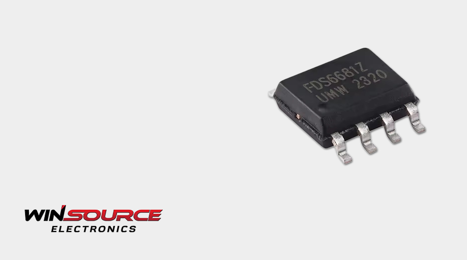
In power management and load control circuits, power MOSFETs are often key components that directly influence system efficiency, thermal stability, and long-term reliability. This is especially true in low- to medium-voltage, high-current applications, where a MOSFET’s conduction performance and switching behavior largely determine overall power dissipation and design margins.
As a mature N-channel power MOSFET, the FDS6681Z has been widely adopted in power path and load control designs due to its balanced performance in conduction loss, thermal behavior, and overall engineering suitability.
1. Device Characteristics and Their Impact on Power System Efficiency
From a structural and parametric standpoint, the FDS6681Z is designed primarily for low- to medium-voltage power systems. Rather than targeting extreme performance figures, its design focus is on optimizing efficiency under typical operating conditions encountered in real-world applications.
Its low R<sub>DS(on)</sub> significantly reduces conduction losses, particularly in continuous conduction or high duty-cycle scenarios. In such applications, lower resistive losses translate directly into improved system efficiency and reduced thermal stress.
In power path control circuits, battery-powered systems, or primary power switching stages, the voltage drop across the MOSFET directly affects the effective output voltage. The low conduction voltage drop of the FDS6681Z allows more usable energy to reach the load while simultaneously reducing device self-heating. This efficiency advantage often results in greater thermal design flexibility, which is especially beneficial for compact PCB layouts.
2. Stability in Load Switching and Power Control Applications
In load switching and power domain management applications, MOSFETs must withstand high transient currents while performing frequent and reliable switching operations.
The advantages of the FDS6681Z in these scenarios are primarily reflected in its stable switching behavior and driver-friendly characteristics.
Its moderate gate charge and drive requirements enable reliable operation with common power management ICs or MCU GPIO-based control, without the need for complex gate driver circuitry. This simplifies system design, particularly in cost-sensitive or space-constrained applications. Additionally, during load transients, inrush events, or startup conditions, the device exhibits predictable electrical behavior, helping to reduce the risk of false triggering or unintended shutdowns.
3. Thermal Performance, Application Scenarios, and System-Level Selection Considerations
MOSFET selection typically requires a balanced evaluation of conduction loss, switching loss, and thermal path design. Even devices with low R<sub>DS(on)</sub> can experience excessive junction temperature rise if package thermal resistance and PCB heat dissipation are not properly matched, especially under high current or long-duration conduction.
The FDS6681Z demonstrates relatively well-balanced thermal performance in commonly used package configurations. With appropriate copper area allocation, thermal via implementation, and current loop design, its temperature rise remains predictable, making it easier to perform power budgeting and thermal margin analysis during the design phase.
From an engineering applicability perspective, and considering both electrical and thermal characteristics, the FDS6681Z is commonly used in the following applications:
- Load switches and reverse polarity protection at DC power inputs
- Synchronous rectification or switching control in low- to medium-power DC-DC converters
- Power domain segmentation and localized power-up control in industrial control boards
- Battery and adapter power path switching in consumer electronics
These applications typically prioritize “adequate specifications, stable behavior, and controllable thermal risk” rather than extreme parameter limits. As a result, while the FDS6681Z is not designed to push maximum performance boundaries, it often delivers a more balanced system-level outcome in terms of efficiency, thermal performance, and design complexity, contributing to smoother validation and more consistent mass production.
During project execution, supply continuity and replacement strategy are also important engineering constraints. Distributors such as WIN SOURCE support engineering teams by providing assistance in part availability, lead-time stability, and component selection, allowing designers to focus more effectively on system design and validation cycles.
© 2026 Win Source Electronics. All rights reserved. This content is protected by copyright and may not be reproduced, distributed, transmitted, cached or otherwise used, except with the prior written permission of Win Source Electronics.

COMMENTS