In modern electronic devices, MOSFETs are widely used in critical circuits such as power management, battery protection, and load switching. Among them, the FDC6312P is a commonly used dual P-channel MOSFET. Thanks to its compact package, relatively low on-resistance, and suitability for low-voltage gate drive, it is widely applied in portable electronic devices, power path control, and DC-DC power systems. However, in practical circuit design, simply understanding the basic specifications of a device is often not sufficient. When using the FDC6312P, engineers must also consider factors such as driving conditions, power dissipation management, and PCB layout in order to ensure circuit stability and efficiency. From a design perspective, this article highlights several key considerations when applying the FDC6312P dual MOSFET in electronic systems.
1. Key Electrical Parameters and Gate Drive Conditions
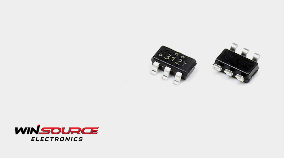
In MOSFET application design, one of the first aspects to consider is the device’s core electrical parameters. The FDC6312P has a typical drain–source voltage (VDS) of -20V, a continuous drain current (ID) of approximately -2A to -2.3A depending on thermal conditions, and is packaged in a SOT-23-6 (SuperSOT-6) package. In most low-voltage power management circuits, these specifications are sufficient to meet common load-control requirements.
In practical designs, the gate–source voltage (VGS) plays a critical role in determining the conduction performance of the MOSFET. The FDC6312P achieves a relatively low RDS(on) when VGS reaches -4.5V, which helps reduce conduction losses. If the gate drive voltage is insufficient, the MOSFET may not fully turn on, resulting in increased resistance and additional heat generation. Therefore, in low-voltage systems such as 3.3V or 5V power environments, engineers must ensure that the driver circuit can provide an appropriate gate voltage.
Attention to gate charge and switching speed is also important. In high-frequency switching applications, insufficient gate drive capability may slow down the MOSFET’s switching process, which can lead to increased switching losses. Therefore, when designing the driver circuit, it is important to select an appropriate gate resistor and properly evaluate the drive capability.
2. Power Dissipation Management and Thermal Design
In power management and load control circuits, MOSFET power dissipation generally comes from two main sources: energy loss during the conduction state and losses during switching transitions. For devices such as the FDC6312P dual P-channel MOSFET, conduction-related heating is often the primary concern in many low-voltage applications. When the load current approaches the device’s rated current, noticeable temperature rise may occur even if the MOSFET has relatively low on-resistance.
Therefore, during the design stage, engineers should evaluate the overall power dissipation of the device based on the expected load current, operating duration, and switching frequency. This ensures that the MOSFET remains within a safe thermal operating range even under worst-case conditions. Ignoring thermal evaluation may lead to excessive junction temperature, which can negatively affect system efficiency, switching stability, and long-term reliability.
The FDC6312P uses a small-form-factor package, which means its inherent heat dissipation capability is limited. To improve thermal performance, several PCB-level optimization strategies can be adopted:
- Increasing the copper area on the PCB to enhance heat spreading
- Using large copper planes or ground layers in multilayer PCBs to assist thermal dissipation
- Avoiding placement of the MOSFET close to other high-temperature components
In battery-powered devices or high-load applications, these thermal management measures are particularly important, as excessive temperature rise can significantly affect MOSFET reliability and lifespan.
3. PCB Layout and Application Design Considerations
Beyond electrical parameters and power dissipation management, PCB layout design also plays an important role in the overall performance of MOSFET-based circuits. For devices such as the FDC6312P dual MOSFET, a well-optimized layout can reduce parasitic inductance and resistance while improving overall system stability and efficiency.
In practical design, the power current path should receive careful attention. Current traces should be kept short and wide to minimize conductor resistance and unnecessary power loss. Particularly in power management circuits, excessively long connections between the MOSFET’s drain and source terminals may introduce additional voltage drop, thereby reducing overall power efficiency. Attention should also be given to the routing of the gate signal. The MOSFET gate is sensitive to noise, and long signal traces or proximity to high-frequency noise sources may cause false triggering or unstable switching behavior. For this reason, engineers typically add an appropriate gate resistor in the gate drive path to suppress oscillations and improve signal stability.
During component selection and circuit implementation, it is also important to carefully verify the pin configuration and internal structure of the device. Although dual MOSFETs from different manufacturers may share similar package formats, their internal structures and pin definitions may differ. Therefore, when designing circuits or selecting replacement parts, the device datasheet should always be consulted to ensure that the circuit connections are correct.
As electronic devices continue to move toward greater miniaturization and higher efficiency, dual P-channel MOSFETs such as the FDC6312P are playing an increasingly important role in power management designs. From gate drive selection and power dissipation control to PCB layout optimization, every design stage can influence the overall performance and reliability of the MOSFET.
In practical applications, engineers should not only focus on the basic device specifications but also consider the surrounding circuit environment and design details. During product development and component sourcing, having access to reliable device information and stable supply channels is equally important. Through professional electronic component distribution platforms, engineers and procurement teams can more efficiently identify suitable MOSFET devices and validate their designs. As one of the global electronic component supply channels, WIN SOURCE offers a wide range of MOSFET products and related resources, helping engineers streamline component selection and accelerate product development.
© 2026 Win Source Electronics. All rights reserved. This content is protected by copyright and may not be reproduced, distributed, transmitted, cached or otherwise used, except with the prior written permission of Win Source Electronics.
COMMENTS