In modern electronic systems, the goal of power design goes far beyond “supplying power.” Engineers must achieve high efficiency, low loss, and reliable thermal management within extremely limited space. As end products continue to shrink, integrating efficient power modules into compact PCB areas has become a major design challenge. Behind these efforts, a small yet high-performance MOSFET — FDG8850NZ — quietly plays a key role in energy conversion.
1. Compact Package, Strong Performance: Core Features of FDG8850NZ
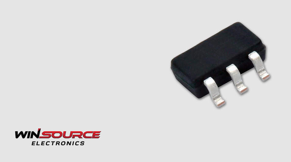
The FDG8850NZ is a dual N-channel MOSFET adopting a compact MicroFET package with a typical size of only 2 × 2 mm. It achieves a balance between low on-resistance (R<sub>DS(on)</sub>) and fast switching speed.
Typical characteristics include:
- R<sub>DS(on)</sub> as low as 0.045 Ω (V<sub>GS</sub> = 4.5 V)
- Wide gate-drive voltage range: 1.8 V to 6 V
- Excellent thermal performance, suitable for high-density layouts
This means that in power modules or portable devices, engineers can significantly improve efficiency and reduce power loss without increasing PCB size.
2. Design Optimization for DC-DC Conversion
In DC-DC converter circuits, efficiency is mainly determined by the combination of conduction and switching losses. The FDG8850NZ adopts a dual-channel integrated structure, allowing it to serve as both the high-side and low-side switches within a single device. This simplifies dual-MOS topologies and shortens current paths.
In synchronous buck configurations, its low R<sub>DS(on)</sub> helps suppress conduction losses. In boost or flyback applications, its fast switching capability supports higher operating frequencies, enabling smaller inductors and capacitors and reducing the overall size of the design. Meanwhile, its symmetrical internal layout ensures both MOSFET channels exhibit highly consistent parameters, which promotes balanced current sharing and thermal stability, improving system efficiency and reliability.
3. Thermal and Reliability Considerations in Compact Designs
For small electronic devices, thermal management often determines product lifespan and stability. The FDG8850NZ provides excellent junction-to-ambient thermal resistance and can maintain a stable junction temperature even in high-frequency DC-DC conversion environments.
Designers can take advantage of its low gate charge (Q<sub>g</sub>) to reduce drive losses, while using proper PCB copper-plane heat dissipation to ensure long-term reliability.
This makes it especially suitable for:
- Smart handheld terminals
- IoT node devices
- Battery-powered sensing modules
- Wearable electronics
4. System-Level Advantages: Efficiency, Simplification, and Scalability
Compared with traditional designs using two discrete MOSFETs, the dual N-channel integration of FDG8850NZ offers multiple advantages:
Simplified layout: reduces routing complexity and parasitic effects between packages;
Efficiency improvement: helps lower conduction and switching losses in synchronous topologies, achieving higher efficiency under proper timing and layout conditions;
BOM cost optimization: reduces component count and matching requirements;
Design scalability: the same package structure can be quickly adapted to different power levels.
In designs emphasizing high efficiency and compact size, the FDG8850NZ, as a small-signal dual MOSFET, provides a cost-effective switching stage solution within limited board space.
5. Application Outlook and Component Selection Guidelines
As wearable, IoT, and mobile devices continue to demand higher energy efficiency, “miniaturization, efficiency, and low power consumption” have become the main development trends for MOSFETs. The FDG8850NZ, a mature and stable device, is widely used in power conversion below 5 V, motor driving, load switching, and lithium-battery protection circuits.
When selecting this component, design engineers can evaluate it based on:
- Power density requirement: recommended continuous drain current ≤ 0.75 A per channel (limited by package power dissipation and thermal design);
- Drive voltage compatibility: supports 1.8 V logic-level drive, suitable for direct MCU control;
- Thermal and assembly capability: MicroFET package enables automated placement and high-density board design;
- In power design, components like the FDG8850NZ are often the “hidden heroes” that quietly enhance overall system competitiveness.
From DC-DC power modules to miniature embedded systems, the FDG8850NZ — with its compact size, low-loss performance, and high integration — brings more efficient energy conversion to modern electronics.
If you are seeking reliable, stable, and production-ready MOSFET components, WIN SOURCE, as a global distributor of electronic components, provides long-term supply and flexible sourcing options for the FDG8850NZ and a wide range of power devices, supporting engineers with efficient and dependable component solutions.
© 2025 Win Source Electronics. All rights reserved. This content is protected by copyright and may not be reproduced, distributed, transmitted, cached or otherwise used, except with the prior written permission of Win Source Electronics.
COMMENTS