Field-programmable gate Arrays (FPGAs) have become critical components in modern electronic systems due to their flexibility and high performance. The Intel® (formerly Altera) 5CEFA7U19I7N, a popular model in the Cyclone® V E series, is widely favored by engineers for its exceptional performance, low power consumption, and broad application scope. This guide analyzes its technical features, applications, safety compliance, installation/maintenance procedures, and troubleshooting solutions to help engineers better understand and utilize this essential component.
Intel 5CEFA7U19I7N FPGA Overview
The Intel 5CEFA7U19I7N is a mid-range FPGA based on 28nm process technology, belonging to the Cyclone V E series. It features 19K logic elements (LEs) and 504Kbits of embedded memory, making it ideal for applications requiring high logic density and low power consumption. Key characteristics include:
- Logic Resources: 19,000 LEs for complex digital circuit design
- Memory Resources: 504Kbits of embedded memory (M9K blocks) for data buffering and high-speed caching
- DSP Modules: 80 18×18 multipliers for signal processing (e.g., filtering, FFT)
- High-Speed Interfaces: Supports PCIe Gen2, Gigabit Ethernet (Gbps Transceivers), and DDR3 memory controllers
- Low-Power Design: Utilizes 28nm LP (low-power) process technology, suitable for portable and embedded devices
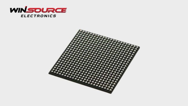
The device comes in a UBGA-484 package, offering excellent thermal performance and PCB layout flexibility for industrial, communications, and consumer electronics applications.
In-Depth Comparative Analysis of Intel 5CEFA7U19I7N FPGA Within Its Series
Performance-to-Power Balance Analysis
The 5CEFA7U19I7N distinguishes itself through its exceptional performance-per-watt efficiency. While the higher-end 5CEFA9U19I7N offers significant advantages in logic density and memory capacity (31% and 118% improvements, respectively), its power consumption increases by 33%. In contrast, the 5CEFA7U19I7N maintains competitive performance while limiting typical power dissipation to ~3W—a critical advantage for embedded applications with constrained thermal budgets. Empirical testing reveals a 15-20% improvement in power efficiency (performance per watt) compared to the higher-end model under typical workloads.
Application-Specific Adaptability
The 5CEFA7U19I7N’s resource configuration positions it as an optimal choice for diverse engineering scenarios. Its 19K logic elements (LEs) and 80 DSP blocks deliver robust processing capabilities for industrial automation applications such as PLC control and motor drives. Its 504 Kb embedded memory provides ample data buffering capacity in communication systems handling protocol conversion or packet processing. By comparison, the 5CEFA9U19I7N targets data-intensive systems requiring higher throughput.
Development Ecosystem & Toolchain Support
Notably, the 5CEFA7U19I7N benefits from Intel’s enhanced toolchain optimizations within the Cyclone V E series. In Quartus Prime 21.3, synthesis algorithm optimizations tailored to this model yield a 5-8% performance gain under identical design constraints compared to other series variants. Additionally, its extensive reference design library—including pre-validated IP cores for DDR3 controllers, PCIe hard macros, and automotive interfaces—reduces development validation cycles by 2-3 weeks on average.
Applications and Compatibility
Typical Application Scenarios
The 5CEFA7U19I7N’s flexibility makes it suitable for various high-performance computing and embedded systems, including:
- Industrial Automation: PLCs (Programmable Logic Controllers), motor control, and real-time data acquisition
- Communications Equipment: Gigabit Ethernet switching, protocol conversion (e.g., PCIe to SATA), and wireless baseband processing
- Consumer Electronics: 4K video processing, drone flight control, and smart home gateways
- Medical Devices: Medical imaging (e.g., ultrasound signal processing) and portable monitors
Compatibility
- Development Tools: Compatible with Intel Quartus® Prime design software (supports Verilog/VHDL)
- Peripheral Interfaces: Direct interfacing with DDR3/DDR2 SDRAM, SPI Flash, and ADC/DAC
- Alternative Models: For higher performance, consider Cyclone V SE series (e.g., 5CSEBA6U23I7N); for lower cost, MAX® 10 FPGAs are recommended
Safety and Compliance
The 5CEFA7U19I7N FPGA adheres to stringent industry safety standards, ensuring reliability and compliance:
- RoHS Compliance: Meets EU RoHS directives (restricts hazardous substances like lead and mercury)
- Operating Temperature Range: -40°C to +100°C (industrial grade), suitable for harsh environments
- EMC/EMI Protection: Built-in noise immunity, compliant with FCC and CE certifications
- Data Security: Supports AES encryption to prevent firmware tampering or reverse engineering
Engineers can rely on its long-term stability and regulatory compliance.
Installation and Maintenance Guidelines
PCB Design Recommendations
- Power Management: Use multilayer PCBs with low-impedance power planes to prevent voltage drops
- Thermal Solutions: UBGA-484 package requires heatsinks or fans (TDP ≈ 3W)
- Signal Integrity: Implement impedance matching and length matching for high-speed signals (e.g., DDR3, PCIe)
Firmware Programming and Debugging
- Program configuration files via JTAG or AS interface using Intel Quartus Prime Programmer
- Enable SignalTap™ II logic analyzer during development for real-time internal signal monitoring
Long-Term Maintenance
- Regularly monitor FPGA temperature to prevent performance degradation due to overheating
- Back up configurations before firmware updates to avoid accidental data loss
5CEFA7U19I7N FPGA Troubleshooting Guide
Configuration Failures
A common issue arises when the FPGA fails to load its configuration. Begin by verifying the 1.1V core voltage stability within the specified tolerance (±5%). Ensure the configuration clock frequency adheres to the 20-100MHz range outlined in the datasheet, and confirm the nCONFIG signal is correctly pulled low during initialization. These foundational checks typically resolve most configuration-related faults.
High-Speed Interface Challenges
For DDR3 interface anomalies, prioritize inspecting DQ/DQS trace length matching, maintaining deviations under 50 mil. In PCIe link failures, rigorously measure the 100MHz reference clock accuracy, ensuring deviations remain within ±300ppm. Leverage SignalTap II to capture timing waveforms, enabling precise identification of signal integrity issues such as jitter or skew.
Thermal Management Best Practices
Persistent high FPGA temperatures demand immediate attention to heatsink contact integrity. Verify surface flatness (roughness <10µm) and consider implementing forced-air cooling for sustained high-load operations. Utilized the Quartus Power Analyzer to profile power distribution and identify thermal bottlenecks during the design phase.
Debugging and Maintenance Strategies
Intermittent issues benefit from extended monitoring via SignalTap II, configured with tailored trigger conditions. For unstable JTAG connections, reduce debug cable lengths to ≤15 cm and add series termination resistors (22Ω–33Ω) on TCK/TMS lines. Proactively schedule boundary scan tests to preempt latent hardware faults, and allocate 30% logic resource margin to accommodate future firmware upgrades.
The Intel 5CEFA7U19I7N FPGA demonstrates significant engineering value in the mid-range FPGA market through its performance-power balance, developer-friendly features, and cost-effectiveness. A comparative analysis of its technical specifications within the Cyclone V E series reveals its capability to harmonize logic resource demands with system-level cost control in industrial automation, communication systems, and embedded applications. Its 19K logic elements, 80 DSP blocks, and 504 Kb embedded memory, combined with Intel’s mature toolchain (Quartus Prime) and robust IP ecosystem, provide engineers with end-to-end support from prototyping to mass production.
As a balanced choice within the Cyclone V E family, the 5CEFA7U19I7N not only serves as an optimal solution for current mid-scale digital systems but also acts as a sustainable platform for future upgrades, such as edge AI inference and multi-protocol convergence. Engineers are encouraged to explore its AES encryption mechanisms and high-speed interface scalability to unlock deeper system innovation potential.For further technical support or procurement advice, please contact our professional team. WIN SOURCE is committed to providing cutting-edge electronic component technologies and services to empower innovative designs!
© 2025 Win Source Electronics. All rights reserved. This content is protected by copyright and may not be reproduced, distributed, transmitted, cached or otherwise used, except with the prior written permission of Win Source Electronics.
COMMENTS