As smart terminals, wearable devices, and environmental sensing systems rapidly evolve, system-level precision is becoming increasingly dependent on the stability of fundamental analog components. Among these, the voltage reference acts as the “anchor” of the entire signal chain. Its performance directly determines the credibility of analog-to-digital conversion.
In portable low-power devices, the voltage reference must not only deliver high accuracy but also meet comprehensive requirements such as ultra-low power consumption, compact size, and strong environmental adaptability. This article focuses on the LT1634BCS8-4.096 voltage reference, providing a systematic analysis of its architectural advantages, key parameters, and integration strategies. Combined with real-world application contexts, we explore the engineering value this device brings to portable electronics.
The Role of Voltage References and the Pressure of Portable Design
The primary task of a voltage reference is to provide a stable and predictable voltage that varies minimally under environmental changes. For modules such as ADCs, DACs, analog front-ends, or sensor bridges, this reference voltage serves as the system’s “measuring stick.” Its accuracy and stability determine output resolution, measurement repeatability, and signal linearity.
In portable systems, the design challenge is multifaceted. On one hand, these systems are battery-powered and highly sensitive to static power consumption. On the other, they are often deployed in outdoor or industrial environments where they must withstand temperature fluctuations and electromagnetic interference. Furthermore, the push for miniaturization limits board space and demands minimal external circuitry. As a result, an ideal voltage reference must strike a delicate balance among accuracy, power consumption, reliability, and ease of integration.
LT1634BCS8-4.096: Key Parameters and Architectural Strengths
The LT1634BCS8-4.096 is engineered specifically for high-accuracy and low-power applications. Its key characteristics include:
- Output Voltage: 4.096 V ±0.05%
Offers precise voltage ideal for ADC reference inputs. Enables full-scale range utilization and improves resolution. - Temperature Coefficient: 20 ppm/°C
Ensures excellent stability across a wide temperature range. Effectively mitigates errors from thermal variation. - Quiescent Current: 60 μA (typical)
Extremely low power consumption. Perfectly suited for battery-powered systems without compromising precision. - Output Drive: ±10 mA
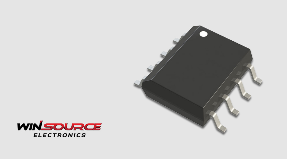
Can drive multiple loads or analog modules. Well-suited for analog chains with moderate load demands. - Package: SOIC-8
A widely-used standard package. Facilitates manufacturing and improves thermal reliability. - Environmental Compliance: RoHS, Pb-Free (#TRPBF)
Meets global environmental regulations. Ideal for industrial and medical applications requiring regulatory compliance.
4.096V: Electrical Advantages and Engineering Fit
Choosing 4.096V instead of traditional 2.5V or 3.0V was a deliberate engineering decision optimized for precision ADC systems. In a 12-bit ADC, the 4096-step resolution aligns perfectly with a 1 mV per-step relationship. This simplifies debugging and software calculations. In 16-bit systems, it supports a wider dynamic range, improves ENOB, and enhances linearity during low-level signal sampling.
The higher reference voltage also allows sensors to output larger signal swings. This reduces the signal chain’s sensitivity to noise and increases the system’s overall signal-to-noise ratio (SNR).
Real-World Value in Portable ADC Systems
In portable acquisition systems built on an MCU and high-resolution ADC, the LT1634BCS8-4.096 plays a critical role as a precision external reference. For example, in wearable health monitors or remote sensor nodes, the system often operates at 3.3V or lower. Internal reference sources typically suffer from offset and drift, which can compromise data consistency. This affects the accuracy of medical evaluations or monitoring algorithms.
As an external reference, the LT1634 offers higher accuracy, superior noise characteristics, and exceptional thermal stability. More importantly, its ultra-low quiescent current enables flexible power management. Even in standby mode, the reference voltage remains stable and ready to support on-demand sampling tasks.
The device also provides excellent power supply rejection (PSRR). This allows it to isolate voltage fluctuations in single-cell lithium or alkaline battery systems and maintain stable output regardless of supply noise.
Comparative Analysis with Common Alternatives
In practical selection, designers often compare the LT1634 against devices like the LM4040AIZ-4.1, ADR3420, or TL431A. The LM4040 offers similar output voltage but suffers from higher temperature drift and over 100 μA quiescent current. Over time, this increases system-level power consumption.
The ADR3420 is optimized for ultra-low power but only outputs 2.048V, which limits ADC dynamic range. The TL431A features adjustable output and strong drive capabilities. However, its typical operating current exceeds 1 mA, making it unsuitable for low-power applications.
In contrast, the LT1634BCS8-4.096 delivers a better overall balance of thermal stability, power consumption, and drive capability. It stands out as one of the most competitive voltage reference options in portable systems today.
Integration Guidelines and Stability Strategies
To fully leverage the LT1634BCS8-4.096, designers should optimize integration from several aspects. First, placing a high-quality ceramic bypass capacitor (0.1 μF to 1 μF) at the output helps suppress high-frequency noise and transient disturbances.
Second, avoid routing its traces near high-frequency switching nodes to prevent EMI coupling. If the input supply exhibits ripple or noise, it is advisable to add a low-noise LDO regulator upstream. This ensures input stability and enhances output accuracy.
In large-scale deployments or harsh environments, further measures such as temperature coefficient binning, aging tests, and dynamic load validation are recommended. These practices help assess long-term consistency and reliability. Such system-level considerations reinforce the voltage reference’s robustness and contribute to consistent product quality in the field.
As the industry moves toward smaller, lower-power, and higher-precision systems, the demands on voltage references are rising. The LT1634BCS8-4.096, with its mature bandgap architecture, carefully tuned thermal characteristics, and proven system compatibility, offers engineers powerful support in meeting these design goals.
It is more than just a voltage source. It forms the bedrock of signal stability across the entire analog signal chain. For high-performance data processing systems, it is a critical engineering enabler that cannot be overlooked.
If you are seeking expert guidance on LT1634 selection, technical documentation, or stable supply solutions, WIN SOURCE offers full-spectrum support. From parameter matching to global logistics, we are committed to helping engineers achieve more efficient and reliable designs.

COMMENTS