As high-speed interfaces such as USB 3.x, HDMI 2.x, and DisplayPort continue to become mainstream, the demand for data transmission quality in electronic systems is steadily increasing. In this context, ESD (Electrostatic Discharge) protection is no longer simply a matter of whether it is implemented, but how to achieve a higher level of protection performance.
The real challenge lies in the fact that introducing ESD protection into high-speed signal paths inevitably affects the signal itself. The core of the design is to achieve a reasonable and controllable balance between protection performance and signal integrity.
1. Hidden Interference in High-Speed Signal Paths
In low-speed systems, the impact of ESD devices on overall performance is typically limited, and meeting basic protection requirements is often sufficient. However, as signal rates increase to the Gbps level, design constraints become significantly more stringent. High-speed differential signals are extremely sensitive to parasitic parameters. Even parasitic capacitance below 1pF introduced by ESD devices can alter signal edge characteristics, degrade eye diagrams, and even lead to bit error risks. These effects are often not apparent at the schematic level but tend to emerge during testing or in real-world operation.
At the same time, the selection of clamping voltage requires careful consideration. If the protection threshold is too high, ESD energy may reach downstream components before the device responds; if it is too low, it may interfere with normal signal transmission. In addition, layout design directly affects protection effectiveness. The distance between the ESD device and the interface determines the discharge path of transient current. If the path is not sufficiently direct, ESD current may impact sensitive nodes within the system before being safely diverted to ground, thereby reducing overall protection efficiency.
2. Selection Is More Than Parameter Comparison
In practical design, selecting an ESD device is not simply a matter of comparing a few parameters, but rather a process of balancing multiple constraints. Particularly in high-speed interface applications, engineers must carefully weigh signal integrity, protection capability, and implementation complexity. Key selection considerations typically include the following:
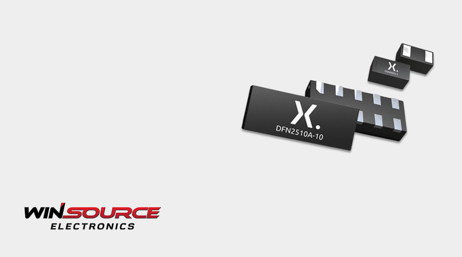
Capacitance
For high-speed interfaces, low capacitance is almost a prerequisite. Parasitic capacitance directly affects signal edges and eye diagram performance, making it essential to minimize interference with the signal path. Devices such as the ECMF06-6AM16, with multi-line ESD array design, provide effective protection while maintaining low impact on high-speed signals, making them suitable for USB and HDMI applications.
Channel Integration
As interface density increases, multi-line ESD arrays are gradually replacing discrete solutions. Compared to multiple single-line devices, array solutions offer advantages in PCB area utilization, routing consistency, and design complexity, while also improving overall design controllability and reducing post-layout debugging efforts.
Response Time
ESD events are characterized by extremely fast, high-energy transients. Devices must respond rapidly to safely divert current to ground; otherwise, protection becomes ineffective.
Leakage Current
In systems sensitive to power consumption or signal bias, leakage current must also be considered. Although typically small, it can have amplified effects in precision applications and should not be overlooked.
3. From Design Decisions to Production Stability
In real-world projects, many designs successfully pass ESD testing in laboratory environments but still encounter issues in actual use. This is often not due to whether protection devices are present, but whether the selection and design truly align with real application conditions. Frequent connector insertion and removal, along with electrostatic accumulation in different environments, introduce a high level of unpredictability to ESD events. Under such conditions, solutions that merely meet parameter requirements may not deliver stable long-term performance. Therefore, ESD device selection should be treated as an early-stage design decision. If the selection is overly conservative or inappropriate at the design stage, later adjustments may involve PCB redesign and potentially impact certification timelines and overall project schedules.
Supply chain considerations must also be taken into account. Although ESD devices are relatively low-cost components, they play a critical protective role. Any disruption in availability or the need for last-minute substitutions may require re-evaluation or revalidation, directly affecting production timelines.
In the context of continuously evolving high-speed interfaces, ESD protection has shifted from being a standard design element to a critical design variable. Multi-line, low-capacitance ESD arrays such as the ECMF06-6AM16 provide engineers with a more balanced solution—offering effective protection without unnecessarily compromising signal performance.
For projects that aim to maintain stability between performance and delivery, both component selection and sourcing reliability are essential. As a professional electronic component distributor, Win Source provides stable inventory support for key components, including ESD protection devices, helping engineering teams minimize uncertainties from design through to mass production.
© 2026 Win Source Electronics. All rights reserved. This content is protected by copyright and may not be reproduced, distributed, transmitted, cached or otherwise used, except with the prior written permission of Win Source Electronics.
COMMENTS