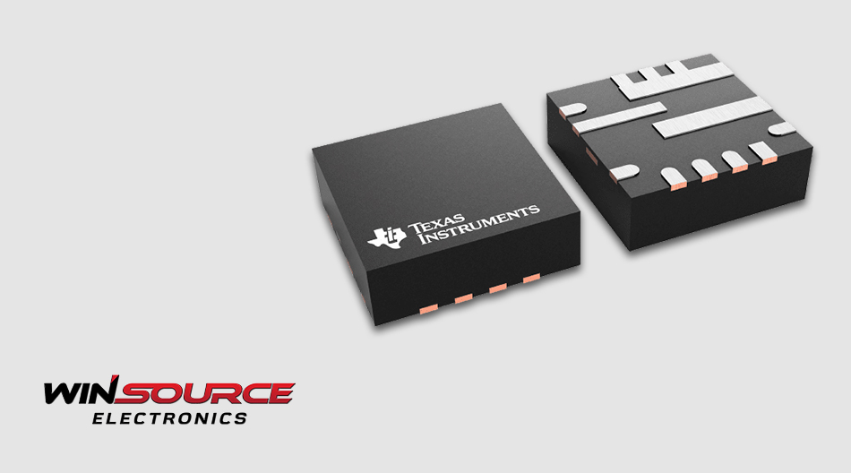
In modern electronic systems, power management ICs play a critical role. As device performance improves and power consumption requirements increase, design engineers need not only a stable power supply but also high efficiency, low noise, and reliable solutions. The TPS56637RPAR from Texas Instruments (TI) is one such synchronous buck DC/DC converter, specifically designed for high-efficiency power conversion. This article takes a deep dive into its operating principle, core architecture, electrical characteristics, and real-world applications to illustrate how it achieves efficient energy conversion.
1. The Concept of a Synchronous Buck Converter
A buck DC/DC converter is one of the most common power topologies, primarily used to step down higher input voltages to lower, stable output voltages. In conventional non-synchronous designs, the circuit typically uses a MOSFET paired with a diode. However, under high-current conditions, the diode introduces significant conduction losses, limiting overall efficiency.
By contrast, the synchronous buck architecture replaces the diode with a low-side MOSFET. This approach greatly reduces conduction losses, improves thermal performance, and enhances overall system efficiency. This architecture lies at the heart of the TPS56637RPAR.
2. Core Architecture of TPS56637RPAR
The TPS56637RPAR is a high-performance power management device from TI. Its internal structure includes several key blocks:
High-Side and Low-Side MOSFETs
The device integrates two MOSFETs for switching and freewheeling. The low-side MOSFET replaces the diode, reducing voltage drop (only a few milliohms Rds(on)), thereby significantly improving efficiency.
PWM Controller
It employs current-mode control combined with Adaptive On-Time (AOT) technology. This ensures fast transient response under load variations while maintaining stable output voltage.
Error Amplifier and Compensation Network
The internal error amplifier compares feedback voltage with a reference voltage and adjusts the duty cycle accordingly. External compensation allows engineers to optimize transient response.
Protection Circuits
Built-in protections include Over-Current Protection (OCP), Over-Voltage Protection (OVP), Under-Voltage Lockout (UVLO), and Over-Temperature Protection (OTP), ensuring reliable operation across demanding environments.
3. Operating Principle
The TPS56637RPAR’s operation can be broken into the following stages:
On-State (Energy Storage)
The high-side MOSFET turns on, allowing current to flow from the input supply through the inductor to the load, causing the inductor current to rise. The low-side MOSFET remains off.
Off-State (Freewheeling)
When the high-side MOSFET turns off, the inductor current continues to flow, now routed through the low-side MOSFET. Because of its very low conduction resistance, this method offers far lower losses than a diode.
Feedback and Regulation
The output voltage is compared with a reference value. The error amplifier adjusts the duty cycle dynamically, ensuring stable voltage regulation.
Light-Load Mode
Under light load conditions, the device can enter pulse-skipping (PFM) mode, reducing switching losses and maintaining high efficiency at low currents.
4. Electrical Characteristics and Design Value
According to TI’s datasheet, the TPS56637RPAR offers:
Input Voltage Range: 4.5 V – 18 V, suitable for various power supply environments.
Output Current Capability: Up to 6 A, ideal for medium- to high-power loads.
Switching Frequency: Adjustable between 200 kHz – 1.2 MHz, providing flexibility in design.
Efficiency: Greater than 90% at 12 V input, 5 V output, and 3 A load.
These features make the TPS56637RPAR highly attractive for industrial control, telecom equipment, server power systems, and automotive electronics.
5. Efficiency and Thermal Considerations
High efficiency not only reduces power loss but also minimizes heat generation. In high-current applications, MOSFET conduction resistance and switching losses are critical. The TPS56637RPAR integrates low Rds(on) MOSFETs and supports high-frequency operation, enabling smaller external inductors and capacitors.
Effective PCB layout—such as enlarging ground copper areas and optimizing thermal vias—further reduces thermal resistance and ensures stable operation under continuous load.
6. Application Examples and Design Tips
When designing with TPS56637RPAR, engineers should consider the following:
Inductor Selection
Choose an inductor with a saturation current at least 30% higher than the maximum load current to prevent saturation.
Input/Output Capacitors
Low ESR capacitors help minimize ripple and improve dynamic response.
PCB Layout
Keep high-current loops short, optimize grounding, and reduce EMI interference.
Thermal Management
Use copper planes and thermal vias, or add heat dissipation measures in high-current applications to maintain safe junction temperatures.
As a high-efficiency synchronous buck converter, the TPS56637RPAR combines advanced architecture, wide input voltage support, and excellent efficiency performance. By understanding its operating principles and key design considerations, engineers can fully leverage its capabilities to achieve reliable, efficient power supply solutions across complex applications.
In an industry increasingly focused on efficiency and reliability, the TPS56637RPAR stands out as a strong choice. For engineers and enterprises looking for reliable sourcing and flexible procurement, WIN SOURCE—one of the world’s leading electronic component distributors—offers TPS56637RPAR and its alternatives with dependable inventory and delivery support, ensuring your projects progress smoothly from design to production.
© 2025 Win Source Electronics. All rights reserved. This content is protected by copyright and may not be reproduced, distributed, transmitted, cached or otherwise used, except with the prior written permission of Win Source Electronics.
COMMENTS