In DC-DC power supply design, MOSFET selection directly impacts conversion efficiency, thermal performance, system stability, and overall reliability. Particularly in portable devices, low-voltage power systems, and space-constrained designs, electrical parameters and package types must be carefully balanced between performance and cost.
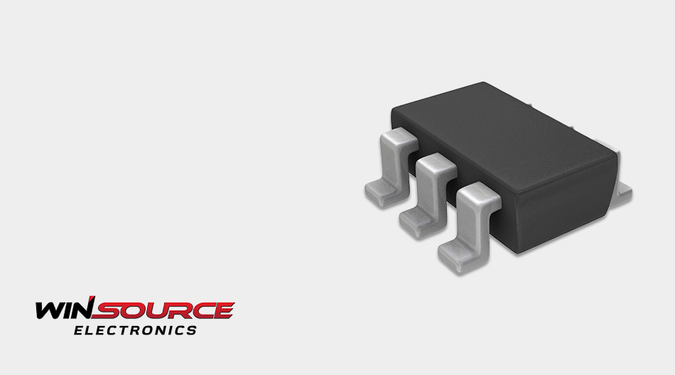
Taking the FDC6312P as an example, this type of P-channel MOSFET represents a typical solution for low-voltage power paths and high-side switching applications. From a system-level perspective, this article discusses its suitability and key design considerations in DC-DC circuits.
1. Core Selection Criteria for MOSFETs in DC-DC Circuits
Voltage Rating and System Margin (Vds)
- The Vds rating must exceed the maximum system input voltage
- Adequate voltage margin should be reserved to withstand transient spikes caused by load changes or parasitic effects
- Excessively high voltage ratings may increase Rds(on), resulting in higher conduction losses
The FDC6312P features a rated drain-source voltage of -20V, making it suitable for low-voltage battery systems or power supply scenarios below 12V. In portable terminals or embedded control board designs, this voltage rating typically provides sufficient safety margin while avoiding efficiency degradation caused by over-specification.
Conduction Performance and Efficiency (Rds(on))
- Rds(on) determines the level of conduction loss
- Under Continuous Conduction Mode (CCM), I²R loss is a primary source of power dissipation
- Lower Rds(on) contributes to higher conversion efficiency and reduced thermal stress
In DC-DC conversion, conduction loss increases proportionally to the square of the load current, making it particularly critical under medium to high load conditions. The FDC6312P achieves low Rds(on) at relatively low Vgs drive levels, making it compatible with logic-level drive environments. This characteristic enables stable efficiency performance in low-voltage control systems while simplifying gate drive design.
By evaluating voltage margin and conduction characteristics together, designers can achieve an optimal balance between safety and efficiency, improving overall DC-DC system performance at the architectural level.
2. Application Suitability of FDC6312P in High-Side and Low-Voltage Systems
In low-voltage DC-DC designs, P-channel MOSFETs are commonly used in high-side switching positions. Compared to N-channel devices, P-channel MOSFETs simplify the drive circuit, as they do not require an additional bootstrap or charge pump driver to achieve full conduction. This advantage is particularly relevant in cost-sensitive or space-constrained designs.
The FDC6312P supports gate-source voltage levels compatible with 3V to 5V logic systems, allowing direct control by MCUs or power management ICs. In battery-powered products such as portable terminals, industrial handheld devices, or IoT modules, high-side P-channel MOSFETs are frequently used for input protection, load switching, or power path management.
Package selection is another important system-level consideration. Compact packages contribute to higher power density but place greater demands on thermal dissipation. During PCB layout, copper area and thermal paths should be optimized to minimize junction temperature rise. For continuous high-current applications, temperature rise calculations based on thermal resistance parameters are recommended, along with appropriate derating under real operating conditions.
3. Design Validation and Supply Chain Considerations
After matching electrical parameters, engineers must also evaluate dynamic performance and long-term reliability. For example, total gate charge (Qg) affects switching losses and EMI behavior. In high-frequency DC-DC topologies, excessive Qg may increase driver losses, while too low Qg can result in voltage overshoot and instability. Therefore, Qg should be assessed in conjunction with switching frequency and driver capability.
Batch consistency and lifecycle management are equally important. For long-term production programs, the supply stability of the selected device should be confirmed, and second-source alternatives should be reserved whenever possible. Although general-purpose low-voltage MOSFETs such as the FDC6312P may have close equivalents across manufacturers, variations in package structure, thermal characteristics, or threshold voltage can affect substitution feasibility. Proper validation is essential.
In practical projects, engineering teams must balance performance, cost, and supply security. System-level evaluation of key parameters, combined with sample testing and thermal simulation, can significantly reduce late-stage redesign risks.
In this context, a stable and reliable component sourcing channel is equally critical. For MOSFETs used in DC-DC power modules, ensuring traceability, parameter transparency, and consistent availability supports a smooth transition from design to mass production. As a global distributor of electronic components, WIN SOURCE offers extensive part resources and supply experience in low-voltage MOSFETs and related power devices, providing support for engineering validation and supply coordination when required.
© 2026 Win Source Electronics. All rights reserved. This content is protected by copyright and may not be reproduced, distributed, transmitted, cached or otherwise used, except with the prior written permission of Win Source Electronics.
COMMENTS