In today’s rapidly evolving electronics landscape — spanning smartphones, wearables, IoT nodes, and portable medical devices — the demand for low-power, high-density, compact power solutions continues to grow. While switching regulators (SMPS) have become increasingly common, low-dropout regulators (LDOs) remain indispensable in scenarios requiring low noise, fast transient response, and ultra-low quiescent current.
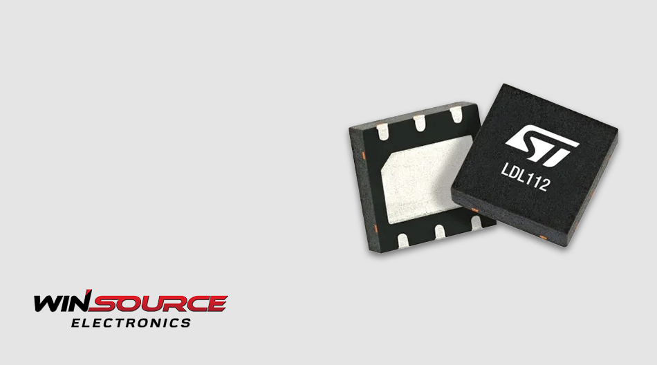
In this article, we focus on STMicroelectronics’ LDL112 series, particularly the LDL112PV33R (3.3 V output, 1.2 A maximum current). We’ll explore its specifications, applications, design considerations, and system integration strategies — revealing why this component stands out as a true low-power LDO champion.
1. Specifications and Key Features
The LDL112PV33R offers an impressive balance between performance and efficiency, with the following key specifications:
Input voltage range: 1.6 V – 5.5 V
Fixed output voltage: 3.3 V; maximum output current: 1.2 A
Typical quiescent current: 35 µA (no load); shutdown current: < 1 µA
Typical dropout voltage: 300 mV at 1 A load; up to 600 mV at full load
Integrated protections: reverse current blocking, overtemperature protection, and current limiting
These characteristics make the LDL112PV33R highly suitable for battery-powered systems and low-voltage environments, minimizing static power loss while maintaining stable output under dynamic load conditions — a hallmark of robust system reliability.
2. Typical Applications and Design Value
Battery-Powered Portable Devices
With an input voltage as low as 1.6 V and ultra-low quiescent current, the LDL112PV33R extends battery life — ideal for handhelds, IoT terminals, and sensor nodes.
Point-of-Load Regulation for MCU / FPGA / DSP
Supporting up to 1.2 A output current, low noise, and reverse current protection, it delivers clean and stable 3.3 V power to logic cores and memory circuits.
System-Level Power Integration
In multi-rail designs where a main switching regulator supplies the primary current rail, the LDL112PV33R serves as an excellent secondary low-noise rail, ensuring fast response and improved performance.
From a value perspective, its combination of low quiescent current (IQ) and moderate output capability positions the LDL112PV33R as a cost-effective and flexible solution for mid-range power designs.
3. Design Recommendations and Best Practices
To fully leverage the performance potential of the LDL112PV33R, consider the following design guidelines:
Input / Output Capacitors
ST recommends ceramic capacitors (CIN and COUT ≥ 1 µF). Pay attention to the capacitor’s ESR characteristics to maintain loop stability.
Enable Pin (EN Control)
Use the EN pin to disable the device during system standby. This reduces power consumption — critical in battery-operated or low-duty-cycle systems.
Thermal Management
At 1.2 A load, internal power dissipation may exceed P = I × (VIN − VOUT). Proper PCB layout and thermal vias are essential to maintain reliability.
Reverse Current Protection
For systems with multiple supply rails or potential reverse bias scenarios, the integrated reverse current blocking feature prevents damage during power transitions.
Transient and Noise Optimization
For noise-sensitive applications (such as ADCs or RF circuits), place output capacitors close to the load and use short, low-impedance traces to enhance transient performance.
4. Design Trade-offs and Challenges
While the LDL112PV33R delivers outstanding efficiency for a linear regulator, engineers should be mindful of a few design trade-offs:
- Despite being a low-dropout device, thermal dissipation increases significantly with higher VIN–VOUT differences and heavy loads.
- Compared with SMPS solutions, efficiency is inherently lower in high-dropout conditions. Systems that demand extreme power efficiency may require hybrid solutions.
- Although quiescent current is low, continuous high-load operation may still challenge thermal limits and require additional cooling measures.
In essence, the LDL112PV33R shines brightest in low-to-medium current, low-noise, and low-IQ applications — not in high-current or ultra-efficiency-driven environments.
5. Industry Trends and Future Outlook
As IoT devices, smart sensors, and edge computing systems evolve, power design faces increasingly demanding requirements — lower standby current, faster transient response, tighter EMC control, and smaller package footprints. Several key trends are shaping the next generation of LDO technology:
- Low-IQ, High-Efficiency LDOs: Hybrid architectures combine low quiescent current with improved efficiency for mixed-supply systems.
- Integrated Protection and Smart Features: Reverse current blocking, output discharge, programmable enable, and status monitoring are becoming standard.
- Miniaturized Packaging: Compact DFN2×2 or similar packages are now favored for mini-IoT and ultra-small modules.
- System-Level Power Coordination: Coordinated operation between LDOs and DC/DC converters optimizes system-level power efficiency and noise performance.
Within this context, the LDL112PV33R — with its low quiescent current, robust 1.2 A output, and integrated protections — represents the direction of intelligent power management for next-generation designs.
Balancing low power, high stability, and integration ease, the LDL112PV33R stands as an ideal solution for a wide range of embedded and portable applications. In real-world design, a power regulator’s selection often determines the overall system performance. Choosing the “right” LDO — not merely an “available” one — ensures the best balance between efficiency, heat dissipation, noise, and reliability.
If your project requires a high-quality, low-power LDO or other power management components, WIN SOURCE provides extensive in-stock availability and professional technical support — helping engineers accelerate design validation and product deployment. Make component sourcing more efficient, and let your innovation focus where it matters most.
© 2025 Win Source Electronics. All rights reserved. This content is protected by copyright and may not be reproduced, distributed, transmitted, cached or otherwise used, except with the prior written permission of Win Source Electronics.
COMMENTS