* Question
What Are the Different Types of Chip Packages and Their Applications?
* Answer
Chip packages play a crucial role in connecting integrated circuits (ICs) to the external environment. They provide mechanical support, protect the chip, and facilitate electrical connections to other components on the circuit board. There are several types of chip packages, each suited for specific applications based on factors like performance, power consumption, space requirements, and manufacturing processes.
Here is a breakdown of the most common types of chip packages and their applications.
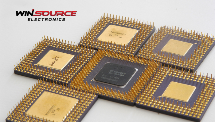
1. Dual In-line Package (DIP)
The Dual In-line Package (DIP) is one of the oldest and most widely used chip packages. It features two parallel rows of pins for electrical connection.
Key Characteristics:
- Pins: Two rows of pins, typically 8 to 40 pins.
- Mounting: Through-hole mounting on the PCB.
- Size: Relatively large, compared to modern packages.
Applications:
- Used in older electronic devices or low-density applications.
- Common in prototyping, as it’s easy to handle and solder.
Why it matters: DIPs are simple, cost-effective, and have been widely used in legacy systems, but they are less efficient in terms of space and performance compared to newer packaging options.
2. Surface-Mount Device (SMD)
Surface-Mount Devices (SMDs) have become the standard for most modern electronics due to their compact size and ease of automation.
Key Characteristics:
- Pins: Mounted directly on the PCB’s surface, with no through-holes.
- Mounting: Soldered onto the surface of the PCB.
- Size: Much smaller than DIPs, allowing for higher pin density.
Applications:
- Used in high-density consumer electronics such as smartphones, computers, and televisions.
- Ideal for automated assembly due to its compact and efficient design.
Why it matters: SMDs allow for smaller, faster, and more reliable electronic devices, making them the preferred choice in most modern applications.
3. Ball Grid Array (BGA)
The Ball Grid Array (BGA) is a high-performance package widely used for devices requiring high I/O counts and excellent thermal performance.
Key Characteristics:
- Pins: The pins are replaced by small solder balls arranged in a grid under the package.
- Mounting: Solder balls are melted to attach the IC to the PCB.
- Size: Smaller footprint and higher pin density compared to traditional packages.
Applications:
- Used in high-performance computing (e.g., CPUs, GPUs, FPGAs).
- Common in mobile devices, servers, and high-speed communication systems.
Why it matters: BGAs offer better thermal management, higher electrical performance, and smaller footprint, making them ideal for complex, high-speed applications.
4. Chip-on-Board (COB)
Chip-on-Board (COB) is a packaging method where the bare chip is directly mounted onto the PCB, eliminating the need for a traditional package.
Key Characteristics:
- Pins: Direct connection to PCB traces, often with wire bonds.
- Mounting: The bare chip is bonded to the PCB with adhesive or solder.
- Size: Ultra-compact, saving significant space.
Applications:
- Used in LED arrays, optical devices, and other applications where space is a premium.
- Common in consumer electronics where space efficiency is crucial.
Why it matters: COB provides a very compact, cost-effective solution for space-constrained applications, though it may require additional considerations for thermal management.
5. Package-on-Package (PoP)
Package-on-Package (PoP) is a method where multiple chip packages are stacked on top of each other to save space and improve performance.
Key Characteristics:
- Pins: Stacked packages with connections between the layers.
- Mounting: Typically uses solder balls or micro bumps for interconnection.
- Size: Space-saving, allowing for high I/O density in a small footprint.
Applications:
- Widely used in mobile devices like smartphones and tablets.
- Used in applications requiring multiple chips, such as memory and logic circuits, to be stacked together.
Why it matters: PoP enables high-performance systems while minimizing board space, making it ideal for compact consumer electronics.
6. Flat Package (QFP, QFN)
Flat Packages like Quad Flat Package (QFP) and Quad Flat No-lead (QFN) are widely used for surface-mount components.
Key Characteristics:
- Pins: QFP has pins on all four sides, while QFN has no leads (just pads underneath).
- Mounting: Soldered onto the PCB’s surface.
- Size: Available in a wide range of sizes with various pin counts.
Applications:
- Common in consumer electronics, automotive, and industrial control systems.
- Used for microcontrollers, ICs, and other peripheral chips.
Why it matters: These packages offer a good balance of performance, ease of assembly, and cost, making them suitable for a wide range of applications.
Engineering Insight: Choosing the Right Package
The choice of chip package depends on various factors:
- Performance: High-speed applications like CPUs or GPUs often require packages like BGAfor better thermal performance and signal integrity.
- Space constraints: For compact consumer electronics or mobile devices, PoPand COB are preferred due to their space-saving nature.
- Cost and ease of assembly: For less complex applications, DIPor SMD packages may be more cost-effective and easier to handle.
Understanding the specific requirements of your application — whether it’s power, size, performance, or cost — is crucial when selecting a chip package.
Conclusion
Chip packaging is a key factor in determining the performance, reliability, and space efficiency of an electronic device. Choosing the right package — from DIP to BGA or PoP — can significantly impact the device’s overall design and functionality. By carefully considering factors like thermal management, electrical performance, and space constraints, engineers can ensure the optimal selection for their circuit designs.
COMMENTS