* Question
How does the charge pump achieve voltage boost?
* Answer
A charge pump is a type of DC–DC converter that boosts (or inverts) voltage without using an inductor.
Instead, it relies on capacitor charging and discharging cycles, controlled by switches or MOSFETs, to transfer energy and create an output voltage higher than the input voltage.
Charge pumps are widely used in display drivers, EEPROM/Flash memory programming, LED biasing, sensor interfaces, and low-power portable devices.
1. Core Principle: Capacitors as Energy Transfer Elements
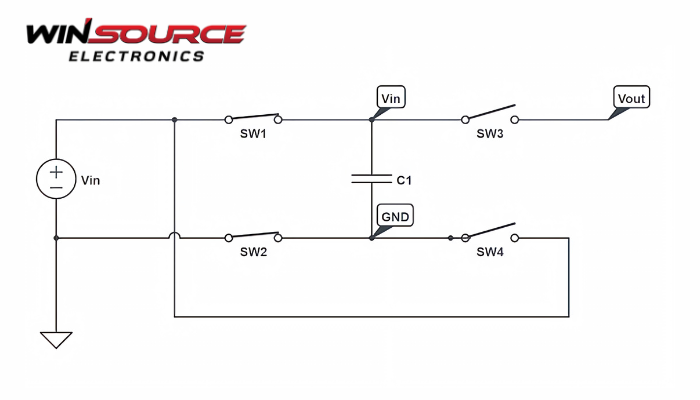
Unlike inductive boost converters, a charge pump works by:
- Storing electrical energy in capacitors
- Reconfiguring capacitor connections using high-frequency switching
- Stacking voltages through charge redistribution
This allows the circuit to produce 2×, 3×, or fractional multiples of the input voltage.
2. Two-Phase Switching Operation
Voltage boosting is achieved through a repeating two-phase switching cycle:
Phase 1: Capacitor Charging
- The flying capacitor Cfis connected directly to the input voltage source.
- It charges up to the input voltage VIN.
Cf→VIN
Phase 2: Capacitor Stacking / Transfer
- Switches reconfigure Cfso that it is placed in series with the input supply.
- The combined voltage appears across the output:
VOUT=VIN+VCf≈2VIN
With additional stages, voltages such as 3VIN or 4VIN can be generated.
This mechanism explains how ICs like the MAX1680 or TPS60241 produce boosted voltages without inductors.
3. Regulation and Control
To maintain a stable output, modern charge pump ICs integrate:
- Oscillatorsto set switching frequency
- Switch driversfor MOSFET control
- Feedback loopsfor voltage regulation
- Bypass or fractional modesto reduce ripple and improve efficiency
For example, a display bias IC such as the LT3469 transitions between 1×/1.5×/2× modes to keep the output voltage stable while minimizing noise.
4. Efficiency Considerations
Charge pump efficiency depends mainly on:
4.1 Capacitor ESR
Lower ESR means lower energy loss during switching.
4.2 Switching Frequency
Higher frequency reduces ripple but may increase switching loss.
4.3 Load Current
Charge pumps are ideal for low to moderate loads; efficiency drops at high current levels.
Because of these characteristics, components like Murata GRM series capacitors are often recommended for their low ESR and stability.
5. Real Engineering Applications
Flash Memory Programming Voltage
Many EEPROM/Flash chips require internal 10–20 V write voltage.
They use an on-chip charge pump (e.g., Microchip 24LC256) to avoid external high-voltage supplies.
LCD Biasing
Display driver ICs use multi-stage charge pumps to generate positive and negative bias rails.
Portable Sensors and Wearables
Charge pumps allow voltage boosting without inductors, reducing EMI and enabling compact PCB layouts.
Conclusion
A charge pump achieves voltage boost by repeatedly charging a capacitor and reconfiguring it in series with the input supply during a second switching phase.
Through controlled switching, capacitors stack voltages to generate higher DC outputs without the need for inductors. This makes charge pumps ideal for compact, low-noise, and low-power electronic systems.
COMMENTS