*Image from the internet; all rights belong to the original author, for reference only.
Table of Contents
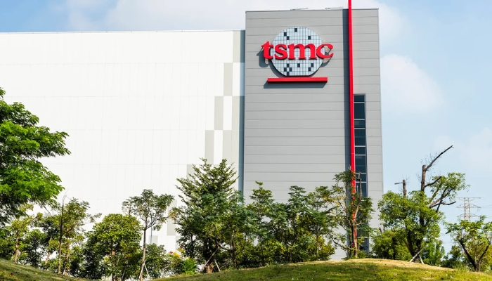
ToggleTSMC Exits 6-Inch Wafer Manufacturing: From Cost Optimization to AI Acceleration — How the Semiconductor Landscape is Being Redrawn
On August 12, 2025, TSMC’s Board of Directors officially approved the withdrawal from its final 6-inch wafer fab and authorized over $20.6 billion USD in capital expenditure. The investment will fund capacity expansions across advanced and mature process nodes, advanced packaging lines, and supporting infrastructure. More than a simple internal restructuring, this strategic move sends a strong message to the industry: the world’s leading foundry is decisively retreating from low-margin legacy processes to fully embrace the AI era by investing in cutting-edge nodes and system-level packaging.
Q1: Why Is TSMC Exiting the 6-Inch Wafer Business?
The primary driver is resource reallocation and profit structure optimization. The 6-inch (150mm) wafer fabs, typically supporting 0.5µm and larger nodes, are associated with low technical barriers and minimal value-add. While they continue to serve analog ICs, power devices (such as MOSFETs), and low-end MCUs—critical in home appliances, industrial control, and consumer electronics—their financial contribution to TSMC has dwindled to less than 0.5% of total revenue.
Legacy components such as the LM393 comparator, IR2104 gate driver, TL431 voltage reference, and NCP1117 voltage regulator, once widely produced on 6-inch lines, will gradually be transitioned to 8-inch nodes or outsourced to foundries specializing in mature processes.
Meanwhile, demand for advanced nodes (5nm/3nm) and heterogeneous integration has exploded due to AI and high-performance computing applications. Repurposing 6-inch fabs into advanced packaging lines (such as CoWoS and SoIC) enhances capital efficiency and better aligns with TSMC’s strategy of high gross margin + high technology barriers.
Q2: Does This Mean TSMC Is Abandoning Mature Nodes?
No. TSMC is not exiting the mature node market entirely but is refining its capacity structure. The company continues to maintain significant 8-inch capacity, supporting demand for mid- to high-end mature products like PMICs, CMOS image sensors, display drivers, and fingerprint recognition ICs.
Notable examples include:
MPQ2483 automotive-grade boost converter
IRF3205S automotive MOSFET
BD9G341AEFJ-LB, a 48V input DC-DC buck converter
These devices will continue to rely on robust 8-inch process lines.
Furthermore, Vanguard International Semiconductor (VIS)—a TSMC affiliate—is expected to take over some legacy 6-inch product lines and enhance its capabilities in the 8-inch PMIC segment, effectively acting as TSMC’s extended arm for mature nodes.
Q3: What Are the Global Implications for the Foundry Market?
This decision will have far-reaching impacts, particularly in the following areas:
1. Customer Redistribution
Small-scale fabless designers and IDM customers—especially those still using 6-inch nodes for Hall sensors, over-voltage protectors, and low-voltage MOSFET controllers in appliances—will be forced to seek alternative foundry partners.
2. Restructuring of Mature Node Resources
Foundries such as UMC, Hua Hong, SMIC, and PSMC—specializing in 8- and 12-inch mature processes—are poised to benefit from increased order inflow and stronger pricing power.
3. IDM Supply Chain Adjustments
Traditional IDM players like TI, STMicroelectronics, and Infineon will need to re-evaluate their foundry strategies, especially for key components like TVS diodes (for ESD protection), CAN transceivers, and automotive-grade MCUs, as they seek to stabilize their supply chain against foundry-side shifts.
Overall, the industry is evolving toward a bifurcated model:
Advanced nodes become increasingly centralized,
Mature nodes become more specialized and distributed.
Q4: What About the Impact on Third-Generation Semiconductors (GaN, SiC)?
The effect is mixed:
GaN (Gallium Nitride)
TSMC previously supported some GaN power and RF devices on 6-inch lines for clients like Navitas and EPC. The transition of these lines into packaging capacity will force those customers to relocate—e.g., the NV6125 GaN half-bridge driver may move to PSMC, Hana Micron, or China Resources Microelectronics.
Short-term tightening of GaN foundry capacity is expected, requiring backfill by niche players.
SiC (Silicon Carbide)
TSMC does not directly operate SiC lines but is partnering via VIS and Episil to build an 8-inch SiC fab, targeting EV fast-charging and industrial power markets.
Examples like C3M0065090K (Wolfspeed) and STP120N10F7 (STMicro) are expected to benefit from this scale-up over time.
Q5: Why Is AI Demand Driving Massive Investment in Advanced Packaging?
As Moore’s Law slows, system-level performance gains can no longer rely solely on transistor scaling. This has elevated advanced packaging to a critical enabler, especially for AI workloads:
Heterogeneous Integration: AI accelerators like GPUs and TPUs must integrate multiple chiplets, high-bandwidth memory (HBM), and PHY interfaces in tightly constrained layouts. Traditional packaging cannot meet the demands for signal integrity, thermal performance, and power density.
CoWoS / SoIC as Key Enablers: TSMC’s CoWoS (Chip-on-Wafer-on-Substrate) technology is now standard for NVIDIA H100, AMD MI300X, and Amazon Trainium 2, with surging demand.
Capacity Bottlenecks: CoWoS capacity is under strain globally. TSMC is facing multi-quarter lead times, making the conversion of 6-inch fabs into packaging lines an urgent and strategic maneuver.
This will further concentrate supply chain control over advanced components such as:
High-speed SerDes interface chips
DDR5 PHY modules
AI orchestration SoCs
Discrete power ICs within HBM stacks
Conclusion: From Legacy Manufacturing to System-Level Ascension
TSMC’s exit from 6-inch wafer production marks more than a routine capacity cleanup—it signals a structural pivot toward a converged future of advanced nodes, system integration, and AI infrastructure. Legacy analog, power, and low-end MCU devices will face short-term disruptions and long-term migration challenges. But this also opens a new era—one defined by precision, performance, and vertical integration.
For the broader supply chain, this transition is both a window of opportunity and a deep-seated recalibration of value in the post-Moore semiconductor age.
© 2025 Win Source Electronics. All rights reserved. This content is protected by copyright and may not be reproduced, distributed, transmitted, cached or otherwise used, except with the prior written permission of Win Source Electronics.
COMMENTS