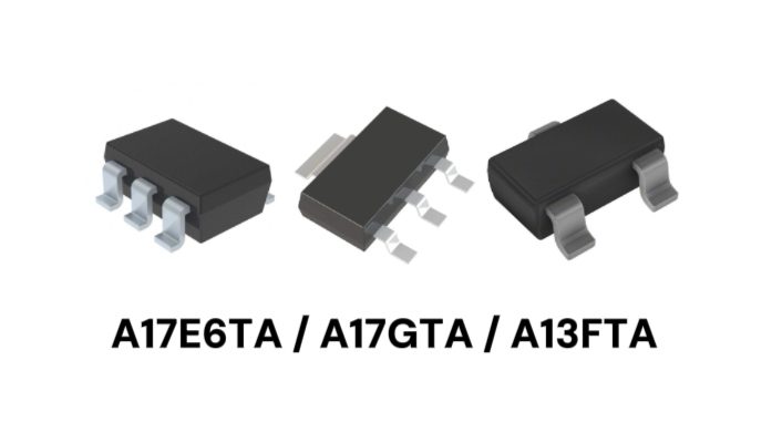
P-Channel MOSFETs are a staple in power management, battery-powered systems, and load switch designs, particularly for high-side switching and power path control. While the ZXMP6A17E6TA, ZXMP6A17GTA, and ZXMP6A13FTA all share the same 60V breakdown voltage, they differ significantly in current handling capability, thermal performance, on-resistance, and intended application. Selecting a device based solely on voltage rating can easily lead to hidden challenges in thermal management, efficiency, or PCB space utilization.
Using the ZXMP6A17E6TA as a reference device, this guide compares it against the ZXMP6A17GTA and ZXMP6A13FTA. By analyzing their specifications, application scenarios, and engineering considerations, we aim to provide practical guidance to help you make the best decision for your specific design constraints.
Parameter Comparison
ZXMP6A17E6TA | ZXMP6A17GTA | ZXMP6A13FTA | |
Drain–Source Voltage (VDS) | 60 V | 60 V | 60 V |
Continuous Drain Current | 2.3 A | 3 A | 0.9 A |
On-Resistance (RDS(on)) | 125 mΩ | 125 mΩ | 400 mΩ |
Max. Power Dissipation | 1.1 W | 2 W | 0.625 W |
Package | SOT-23-6 (SOT-26) | SOT-223 | SOT-23-3 |
Typical Positioning | Compact, medium-power switch | High power, enhanced thermal performance | Light load, space-constrained designs |
Application Analysis
ZXMP6A17E6TA
Ideal For: Power path management in battery-powered devices, on-board load switching, and handheld instruments.
Analysis: Delivering an on-resistance (125 mΩ) comparable to the larger SOT-223 but within a compact SOT-23-6 footprint, this device strikes an optimal balance between size and performance. For portable terminals or modular designs, it conserves valuable PCB real estate while comfortably handling continuous currents around 2A, effectively minimizing the need for auxiliary thermal management.
ZXMP6A17GTA
Ideal For: Industrial control I/O, motor drive input stages, LDO input circuits, and high-temperature environments.
Analysis: The SOT-223 package features a larger metal tab, resulting in significantly lower thermal resistance compared to the SOT-23 series. In industrial applications requiring continuous conduction, operation in harsh environments, or superior thermal stability, the ZXMP6A17GTA dissipates heat into the PCB more efficiently, ensuring long-term system reliability.
ZXMP6A13FTA
Ideal For: Wearables, IoT sensor nodes, portable instrumentation, and signal switching.
Analysis: This model is engineered for light-load, intermittent operation, or ultra-space-constrained applications. While its on-resistance is higher (~400 mΩ), voltage drop and power loss remain negligible at microamp or milliamp load levels. It fulfills basic switching requirements with a minimal PCB footprint, enabling higher integration in high-density board designs.
Design Considerations
Gate Drive Stability in High-Side Switching
When using a P-Channel MOSFET as a high-side switch, the device only conducts when the gate voltage is lower than the source voltage. During system power-up, power-down, or when the MCU GPIO is in a high-impedance (High-Z) state, a pull-up resistor between the gate and source is mandatory. This ensures the MOSFET defaults to an OFF state, preventing accidental load activation or undefined system behavior.
Thermal Management & PCB Layout
Thermal failure is often a result of suboptimal layout rather than device limitations.
For the ZXMP6A17GTA: Maximize the copper pour area connected to the drain pin to act as a heatsink.
For the E6TA and FTA: Due to their compact packages, avoid placing them near significant heat sources (such as CPUs or high-current inductors) to prevent thermal coupling, which can derate their performance.
Conduction Loss Evaluation
Do not use the ZXMP6A13FTA for continuous loads exceeding 0.5A.
Due to its higher on-resistance, driving currents near 1A will result in significant voltage drop and excessive heating. For loads approaching or exceeding 1A, select the E6TA or GTA models to maintain efficiency and thermal safety margins.
Protection Against Inductive Loads
When driving inductive loads such as relays or motors, the back EMF (voltage spike) generated during turn-off can exceed the MOSFET’s breakdown voltage. It is critical to place a freewheeling diode in parallel with the load or add a TVS diode across the drain and source to clamp these spikes and protect the switch.
Replacement & Migration Recommendations
ZXMP6A17E6TA ↔ ZXMP6A17GTA
Electrical Performance: Both models share identical on-resistance and possess very similar electrical characteristics, ensuring consistent performance across both packages.
Migration Strategy: If the E6TA exhibits excessive temperature rise in your application, migrating to the GTA is recommended to improve heat dissipation. Conversely, if the system requires a smaller form factor and has ample thermal headroom, the E6TA can serve as a compact alternative to the GTA. Please note that the PCB footprints are incompatible (SOT-23-6 vs. SOT-223), so switching between them requires a board layout redesign.
ZXMP6A17E6TA ↔ ZXMP6A13FTA
Positioning Difference: The FTA is strictly designed for low-current applications, whereas the E6TA handles medium loads.
Migration Strategy: Consider replacing the E6TA with the FTA only if the load current is minimal (<500mA) and the design prioritizes ultra-low cost or space savings. On the other hand, if an existing FTA design is overheating or suffering from voltage sag, upgrading to the E6TA is the most direct and effective solution.
Collectively, the ZXMP6A17E6TA, ZXMP6A17GTA, and ZXMP6A13FTA address a broad spectrum of design requirements—from compact medium-power switching and high-power thermal control to low-power, light-load tasks. In the selection process, engineers should avoid relying on a single parameter. Instead, evaluate the system load characteristics, board space constraints, and thermal design limits to define priorities. By matching the specific device to its intended scenario, you can achieve an optimal balance between reliability, efficiency, and scalability.
Key Takeaways
ZXMP6A17E6TA: Compact Size, Low Resistance
ZXMP6A17GTA: Superior Thermals, Robust Design
ZXMP6A13FTA: Minimal Footprint, Cost-Optimized
WIN SOURCE provides reliable supply and technical support for the complete ZXMP6A P-Channel MOSFET series. Whether you are designing ultra-compact wearables or high-reliability industrial power systems, we help you find the optimal balance between performance and supply chain stability. Visit WIN SOURCE today for real-time inventory and pricing.
©2025 Win Source Electronics. All rights reserved. This content is protected by copyright and may not be reproduced, distributed, transmitted, cached or otherwise used, except with the prior written permission of Win Source Electronics.

COMMENTS