In clock design, component selection is not only about matching the required output frequency. It also affects system synchronization, signal integrity, PCB implementation, and long-term supply stability. PL502-37QC-R is a VCXO / clock multiplier device that supports a 12–25 MHz crystal input and a 0.75–800 MHz LVCMOS output. It is offered in a 16-QFN / WFQFN exposed pad package. For legacy project maintenance, BOM replacement, or supply chain verification, engineering teams should also confirm the complete part number, package, temperature grade, lifecycle status, and traceability to avoid making selection or replacement decisions based only on core frequency specifications.
1. Device Positioning and Key Selection Considerations
PL502-37QC-R is a VCXO / clock multiplier device suitable for board-level systems that require a stable clock source, frequency synthesis, or clock multiplication. Because clock devices can directly affect system synchronization, data transmission stability, and timing margin, engineers should not evaluate the device based only on output frequency. They should also review the crystal input frequency, output range, LVCMOS logic level, supply voltage, temperature grade, package size, and the target application’s jitter and phase noise requirements.
During product introduction or replacement evaluation, the complete part number and its suffixes should also be verified. In PL502-37QC-R, the “C” suffix corresponds to a commercial temperature grade, while “-R” generally indicates Tape & Reel packaging. Therefore, similar part numbers should not be treated as direct replacements based only on the same prefix. For legacy project maintenance, BOM replacement, or new design-in decisions, engineers should further confirm the manufacturer lifecycle, current supply status, lot information, and long-term availability risks. This helps avoid procurement or production issues caused by differences in package, temperature grade, packaging format, or supply status.
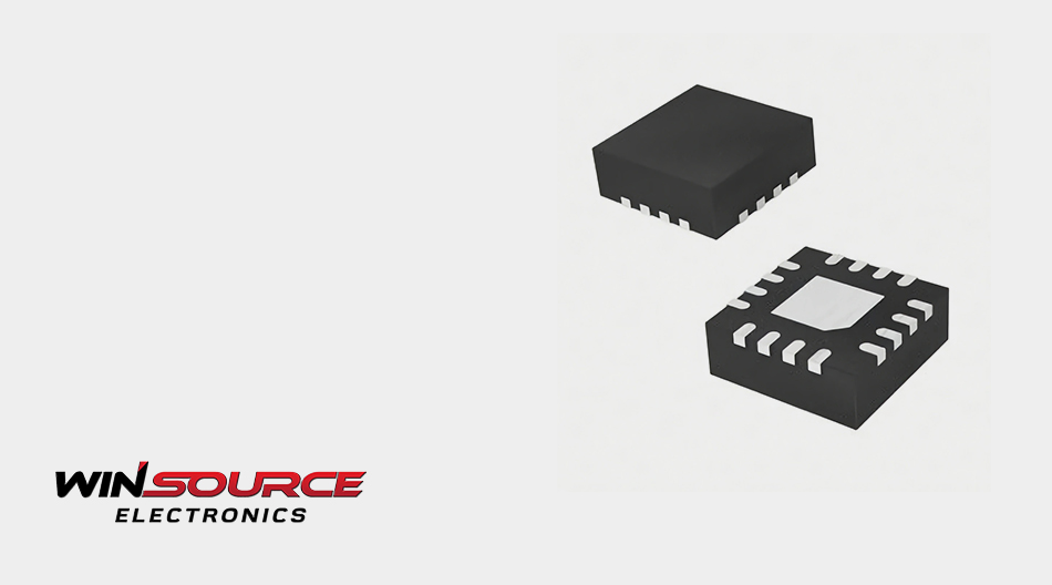
2. How the 16-QFN / WFQFN Exposed Pad Package Affects Selection
PL502-37QC-R is offered in a 16-QFN / WFQFN exposed pad package. Compared with traditional leaded packages, this small leadless package helps save PCB space and is suitable for board-level systems with space constraints or high-density layouts. However, package size compatibility is only the first step in the selection process. Engineering teams also need to evaluate whether the existing PCB footprint, assembly process, and inspection conditions can support this package reliably.
In legacy project maintenance or BOM replacement scenarios, package compatibility becomes even more important. Even when the device function and frequency range appear similar, differences in the land pattern, exposed pad size, pad layout, or package height may still affect soldering quality and assembly results. For this reason, replacement evaluation should include a comparison between the original PCB footprint and the target device package documentation. Engineers should avoid assuming that a device is a direct replacement based only on package names such as “16-QFN” or “WFQFN.”
In addition to outline dimensions, the exposed pad connection should also be confirmed in advance. Its size, soldering requirements, and electrical connection should follow the manufacturer’s documentation. Exposed pads should not be assumed to function as ground connections by default. If the existing PCB connects the bottom pad to the ground plane or uses a via-in-pad design, engineers should further verify whether that structure meets the package requirements of PL502-37QC-R and whether it is compatible with the available assembly capability.
Therefore, package evaluation for PL502-37QC-R is not about adding unnecessary PCB design complexity. The key is to confirm whether the device fits the existing board-level design, manufacturing capability, and assembly process. For new designs, the manufacturer-recommended footprint can be planned in advance. For replacement introduction, engineers should first check whether there are differences in footprint, exposed pad design, soldering inspection conditions, and packaging format.
3. Power Integrity and Clock Routing Control
As a VCXO / clock multiplier device, PL502-37QC-R is relatively sensitive to power supply noise and PCB routing conditions. In layout design, decoupling capacitors should be placed close to the power pins. The return path from the capacitor to the device pins and ground plane should be kept as short as possible. The specific capacitor values and combinations should be determined based on the datasheet, reference design, and overall board-level power noise conditions. Engineers should avoid directly reusing the peripheral configuration of other clock devices without verification.
Clock signals should maintain a continuous, low-impedance reference plane. They should avoid crossing ground plane splits or discontinuous reference layers to reduce the risk of impedance discontinuity, crosstalk, and EMI. For LVCMOS outputs, engineers should evaluate whether a series resistor should be reserved near the output pin based on output frequency, trace length, receiver load, and system EMI requirements. In multi-load scenarios, a dedicated clock buffer may also be considered.
The crystal should be placed close to the XIN / XOUT pins, and the related traces should be short and compact. They should also be kept away from switching power supply nodes, high-speed digital traces, and high-current paths. The PL502-37 series typically does not require an external load capacitor or varicap. If the crystal network needs to be adjusted due to crystal specifications, legacy board compatibility, or special tuning requirements, engineers should first review the datasheet and actual circuit conditions. The impact on pull range, startup behavior, and frequency stability should be evaluated before making changes.
4. Procurement Verification and Engineering Validation Recommendations
During procurement and product introduction for PL502-37QC-R, engineering teams should verify more than the part number itself. They should also confirm the package type, packaging format, Date Code, Lot Code, supply status, lifecycle status, and traceability. For legacy project maintenance, repair replacement, or high-reliability applications, lot information, storage conditions, and moisture sensitivity level management may also affect downstream assembly and validation processes.
If the device is used for legacy project continuation or replacement evaluation, the team should first determine whether the current BOM requires an exact match to PL502-37QC-R, or whether a same-series, functionally equivalent, or newer-generation alternative can be accepted. Replacement evaluation should not be based only on the output frequency range. It should also include crystal input requirements, control voltage range, output logic, supply voltage, package compatibility, temperature grade, control pin definitions, and PCB footprint consistency.
Overall, the selection focus of PL502-37QC-R is not limited to frequency range and package compatibility. It also depends on whether the device matches the system clock architecture, PCB manufacturing capability, assembly process, and long-term supply requirements. For clock devices using a 16-QFN / WFQFN exposed pad package, early footprint review, layout risk assessment, lifecycle confirmation, and procurement information verification can help reduce risks in later debugging, replacement, and production stages. In BOM management, replacement evaluation, or supply chain verification, WIN SOURCE can assist customers with part number confirmation, package verification, supply status checks, and lot information review for clock devices such as PL502-37QC-R, providing engineering and procurement teams with more complete selection and sourcing references.
©2026 Win Source Electronics. All rights reserved. This content is protected by copyright and may not be reproduced, distributed, transmitted, cached or otherwise used, except with the prior written permission of Win Source Electronics.
COMMENTS