
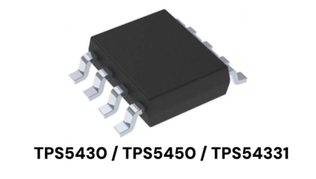
TPS5430MDDAREP, TPS5450MDDAREP, and TPS54331DDAR are all nonsynchronous buck converters with an integrated high-side MOSFET. Each device requires an external catch diode to provide the low-side current path. Although they are often compared within the same power-supply category, they should not be treated as simple “36 V/3 A, 36 V/5 A, and 28 V/3 A” current tiers.
For engineering selection, the more meaningful differences are product grade, control and compensation architecture, light-load behavior, minimum on-time, startup and protection features, current-limit boundaries, and pin compatibility.
Parameter Comparison
| Parameter | TPS5430MDDAREP | TPS5450MDDAREP | TPS54331DDAR |
| VIN operating range | 5.5 V to 36 V | 5.5 V to 36 V | 3.5 V to 28 V |
| Output current | 3 A continuous; 4 A peak | 5 A continuous; 6 A peak | 3 A continuous |
| Control mode | Voltage-mode control with input feedforward | Voltage-mode control with input feedforward | Peak current-mode control |
| Compensation | Internal Type III compensation | Internal Type III compensation | External Type II compensation |
| Switching frequency | 500 kHz; 400 to 600 kHz | 500 kHz; 375 to 600 kHz over temperature | 570 kHz typical; 456 to 684 kHz at 12 V, 25°C |
| High-side MOSFET RDS(on) | 110 mΩ typical; 230 mΩ maximum | 110 mΩ typical; no guaranteed maximum | 80 mΩ typical; 150 mΩ maximum at 12 V |
| Feedback reference / minimum on-time | 1.221 V / 200 ns maximum | 1.221 V / 220 ns maximum | 0.8 V / 130 ns maximum |
| Light-load and startup control | Can enter DCM; approximately 8 ms internal soft-start | Can enter DCM; approximately 8 ms internal soft-start | Eco-mode; adjustable soft-start and UVLO |
| Current-limit threshold | 4 to 8.5 A | 4.4 to 11.7 A over temperature | 3.5 to 5.8 A at 12 V |
| Junction temperature / product grade | -55°C to 125°C; Enhanced Product | -55°C to 125°C; Enhanced Product | -40°C to 150°C; Catalog device |
| Package / compatibility | DDA-8; same pinout as TPS5450-EP | DDA-8; same pinout as TPS5430-EP | DDA-8; different pinout, not a direct replacement |
Application Analysis
- TPS5430MDDAREP
TPS5430MDDAREP is primarily positioned as a 3-A Enhanced Product buck solution for controlled 12-V and 24-V buses. Its main advantages are a mature fixed architecture, internal compensation, a wide input-voltage range, and product attributes that are well suited to industrial programs and long-term supply management.
- Best suited for: Controlled 12-V or 24-V input systems; 5-V, 3.3-V, and other low-to-mid-voltage rails; continuous load current up to 3 A; projects requiring a -55°C to 125°C junction-temperature range; and designs that value Enhanced Product qualification, a controlled baseline, and more stable lifecycle management.
- Design note: Because the device uses internal compensation, the output inductor and capacitor cannot be changed arbitrarily. Replacing conventional electrolytic or polymer capacitors with an all-ceramic output network changes the ESR zero, effective capacitance, and transient energy storage. Loop stability and load-transient response must therefore be revalidated.
- TPS5450MDDAREP
TPS5450MDDAREP shares the same package, pinout, control architecture, and Enhanced Product classification as TPS5430MDDAREP. It is therefore the most direct candidate when an existing TPS5430-EP platform needs to be extended toward a 5-A output. However, it is not an IC-only swap that automatically delivers more current. A 5-A rating materially increases stress on the catch diode, inductor, input and output capacitors, PCB copper, and thermal structure.
- Best suited for: Existing TPS5430-EP platforms that need to move from 3 A toward the 3-A-to-5-A range; systems requiring additional transient-load margin; designs where the catch diode, inductor, capacitors, PCB copper, and thermal solution can be updated; and projects that still require Enhanced Product grade and wide-temperature capability.
- Design note: The high-side MOSFET RDS(on) remains approximately 110 mΩ typical, while the upper end of the current-limit range reaches 11.7 A over temperature. Recalculate normal operating temperature rise, short-circuit stress, inductor saturation current, diode thermal capacity, and the PCB heat-flow path.
- TPS54331DDAR
TPS54331DDAR trades a lower 28-V input ceiling for greater design flexibility through peak current-mode control, external compensation, Eco-mode operation, and adjustable soft-start and UVLO. Compared with TPS5430-EP and TPS5450-EP, it is generally better suited to systems that prioritize light-load efficiency, lower output voltages, and output-filter optimization.
- Best suited for: 5-V and 12-V bus systems; 24-V systems whose worst-case input is reliably held below 28 V; equipment that spends long periods at light load or standby; designs requiring adjustable soft-start, adjustable UVLO, or low shutdown current; and applications that use all-ceramic output capacitors with compensation designed around the actual filter network.
- Design note: The external COMP pin provides greater loop-design freedom, but also places compensation calculation and validation on the designer. Eco-mode improves light-load efficiency, yet it may change light-load ripple and the noise spectrum. Systems sensitive to analog noise, supply ripple, or EMI should be verified with bench measurements.
Design Considerations
- TPS5450-EP does not provide a “free” extra 2 A
For a 24-V-to-5-V conversion, the catch diode conducts for approximately 79% of each switching cycle. Assuming VF = 0.5 V, diode loss is about 1.2 W at a 3-A load and about 2 W at a 5-A load. The higher current rating expands the IC operating range; it does not automatically upgrade the catch diode, inductor, output capacitor, or thermal structure.
- Evaluate a 24-V bus at the worst-case transient voltage
The maximum operating input voltage is 36 V for TPS5430MDDAREP and TPS5450MDDAREP, but only 28 V for TPS54331DDAR. A 24-V bus must be assessed beyond its nominal steady-state voltage. Include supply tolerance, hot-plug events, cable-inductance spikes, TVS clamp variation, and PH-node overshoot. TPS54331DDAR has limited headroom on a 24-V bus and should be used directly only when the worst-case input is reliably constrained below 28 V.
- Internal compensation limits output-filter freedom
TPS5430MDDAREP and TPS5450MDDAREP use internal Type III compensation, so the inductor and output-capacitor combination cannot be changed freely. Moving from electrolytic or polymer capacitors to an all-ceramic network changes ESR, effective capacitance, ripple, and transient response, which can affect loop stability. TPS54331DDAR provides an external COMP pin and is better suited to compensation designed around the actual inductor, capacitor, and ESR conditions.
- The feedback reference is not the minimum practical output voltage
The feedback reference is approximately 1.221 V for TPS5430MDDAREP and TPS5450MDDAREP and approximately 0.8 V for TPS54331DDAR. At high input voltage, however, the minimum achievable output is also constrained by minimum on-time, switching frequency, diode drop, MOSFET on-resistance, inductor DCR, and load conditions. Low-output-voltage applications, especially 24 V to 1.8 V or 1.2 V, should be rechecked at maximum VIN, maximum switching frequency, and temperature corners. A synchronous buck converter may be the better choice.
- Use current-limit specifications for fault-stress analysis, not continuous output rating
All three data sheets specify a current-limit range, but this parameter is primarily intended for protection and fault-stress analysis. It should not be interpreted as sustainable output capability. Under the worst-case current limit, verify inductor saturation, peak-current and thermal stress on the catch diode, and the energy imposed on the input source, PCB traces, and output capacitors during a short circuit or repeated restart sequence.
- The same DDA-8 package does not mean a direct replacement
Although TPS54331DDAR also uses a DDA-8 package, only BOOT (pin 1) and PH (pin 8) are in the same locations. The functions or positions of the remaining pins differ from TPS5430/TPS5450. In addition, TPS54331DDAR requires a 0.1 μF BOOT capacitor, whereas TPS5430/TPS5450 use 0.01 μF. The three devices are therefore not directly interchangeable.
Selection Recommendations
- Choose TPS5430MDDAREP for a controlled 12-V/24-V bus, 5-V or 3.3-V output, load current up to 3 A, and Enhanced Product supply-chain requirements.
- Choose TPS5450MDDAREP when an existing TPS5430-EP platform must be extended toward 3 A to 5 A and the diode, inductor, capacitors, PCB copper, and thermal design can be updated.
- Choose TPS54331DDAR when worst-case input remains below 28 V and the design benefits from low shutdown current, adjustable soft-start/UVLO, long light-load operation, and flexible loop optimization.
- Evaluate a higher-voltage synchronous buck converter for direct 24-V conversion to 1.8 V or 1.2 V, or when efficiency and thermal performance are primary design constraints.
Product Summary
| Part Number | Manufacturer | Core Positioning | Buy |
| TPS5430MDDAREP | Texas Instruments | Controlled 12-V/24-V buses, loads up to 3 A, and Enhanced Product supply requirements | Buy Now |
| TPS5450MDDAREP | Texas Instruments | TPS5430-EP platform extension to 5 A, with a redesigned power stage and thermal solution | Buy Now |
| TPS54331DDAR | Texas Instruments | Light-load efficiency, adjustable startup/UVLO, and flexible output-filter design | Buy Now |
WIN SOURCE provides inventory support, lifecycle analysis, BOM cross-reference services, and alternative sourcing support for TI power-management ICs, buck converters, and complementary power components. Visit WIN SOURCE to check real-time inventory for the TPS5430MDDAREP, TPS5450MDDAREP, TPS54331DDAR, and other critical power devices, then select a sourcing solution based on application conditions, stock status, quality grade, and actual circuit compatibility.
©2026 Win Source Electronics. All rights reserved. This content is protected by copyright and may not be reproduced, distributed, transmitted, cached or otherwise used, except with the prior written permission of Win Source Electronics.

COMMENTS