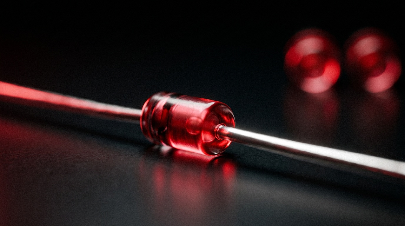
The Zener diode is one of those components that looks unremarkable on a schematic but quietly handles some of the most important work in a circuit. While a standard diode is designed to block reverse current, the Zener is built to embrace it — conducting in reverse at a precise, predictable voltage and holding that voltage steady even as conditions around it change. That single property is the foundation of voltage regulation, overvoltage protection, signal clipping, and stable voltage references across virtually every category of electronic design.
This article explains how Zener diodes work from first principles, walks through the key specifications you’ll encounter on a datasheet, covers the most common applications, and provides a practical framework for selecting the right part for a given circuit. Whether you’re designing a new power supply, protecting an ADC input, or sourcing a replacement for an existing design, the goal here is to give you a clear and usable understanding of what a Zener diode actually does and how to choose one with confidence.
What Is a Zener Diode?
What Is a Zener Diode?l,Helvetica,sans-serif;font-size:12pt">A Zener diode is a two-terminal semiconductor device — a heavily doped P-N junction — specifically designed to operate in its reverse breakdown region without sustaining damage. Ordinary silicon diodes are not built for this; push them beyond their reverse breakdown voltage and they typically fail. Zener diodes are manufactured to not only tolerate that breakdown point but to exploit it. Once the reverse voltage across the device reaches the rated Zener voltage (VZ), current flows freely in reverse while the voltage across the diode terminals remains essentially constant. That clamped, stable voltage is what makes the Zener diode valuable.The device is named after physicist Clarence Zener, who described the quantum mechanical tunneling effect behind low-voltage breakdown in 1934. Modern Zener diodes are available in a wide range of breakdown voltages — typically from around 1.8 V up to 200 V or more — and in power ratings from a fraction of a watt to tens of watts. In circuit diagrams, the Zener is represented by a standard diode symbol with a bent or Z-shaped line at the cathode end, indicating its ability to conduct in both directions under the right conditions.
How Zener Diodes Work
How Zener Diodes Workfamily:Arial,Helvetica,sans-serif;font-size:14pt;margin-top: 30px;margin-bottom: 15px">Forward Bias Behavior
Forward Bias Behaviorica,sans-serif;font-size:12pt">In forward bias — with the anode connected to the more positive voltage — a Zener diode behaves exactly like a standard silicon diode. It begins conducting once the forward voltage exceeds roughly 0.6–0.7 V, maintaining a small, stable voltage drop across its terminals. This forward-bias behavior is unremarkable and is not what Zener diodes are typically selected for, though it can occasionally be useful in certain circuit configurations.
Reverse Bias and the Breakdown RegionReverse Bias and the Breakdown Region
ns-serif;font-size:12pt">The interesting behavior happens in reverse bias. As reverse voltage across the diode increases from zero, only a very small leakage current flows — the diode is effectively blocking, just like a standard rectifier diode. But once the reverse voltage reaches VZ, the breakdown voltage specific to that part, something changes sharply. The impedance of the diode drops dramatically, and current can flow freely in the reverse direction. Crucially, even as that reverse current varies over a wide range, the voltage across the diode stays nearly constant at VZ. This is the defining characteristic: a Zener diode in breakdown acts as a voltage clamp.This behavior is not destructive, provided the current is limited so that power dissipation stays within the rated maximum. A series resistor is almost always used in practice to prevent the Zener from drawing unlimited current from the source, which would exceed its power rating and destroy the device.
The Two Breakdown Mechanisms
The Two Breakdown Mechanisms-serif;font-size:12pt">Two distinct physical mechanisms produce the reverse breakdown behavior in Zener diodes, and which one dominates depends on the rated voltage of the device.
Zener breakdown (quantum tunneling) occurs in heavily doped diodes at lower voltages, generally below about 5 V. The strong electric field across the narrow depletion region allows electrons to tunnel directly from the valence band of the P-type material into the conduction band of the N-type material — bypassing the potential barrier rather than jumping over it. This mechanism has a negative temperature coefficient: the breakdown voltage decreases slightly as temperature rises.
Avalanche breakdown is the dominant mechanism at higher voltages, typically above 6 V. Here, minority charge carriers accelerated by the electric field collide with lattice atoms, generating additional electron-hole pairs through impact ionization. Those new carriers are themselves accelerated and cause further collisions, creating a chain reaction that produces a sharp rise in current. Avalanche breakdown has a positive temperature coefficient — breakdown voltage increases with temperature.
Around 5–6 V, both mechanisms are active and their opposing temperature effects partially cancel each other out, making parts in this voltage range exhibit near-zero temperature coefficient and the best thermal stability. This is why diodes rated at approximately 5.6 V are frequently chosen for precision voltage reference applications where temperature stability matters.
How a Zener Diode Regulates Voltage
How a Zener Diode Regulates Voltage;font-size:12pt">The most fundamental Zener diode circuit is the shunt regulator. The Zener is placed in parallel with the load, with a series resistor between the unregulated supply and the Zener/load junction. The cathode of the Zener connects to the positive rail; the anode connects to ground. When the supply voltage exceeds VZ, the diode enters breakdown and conducts. Any excess voltage appears across the series resistor rather than across the load, and the output voltage is clamped at VZ.
What makes this useful is that it handles both input voltage variations and load current changes. If the input voltage rises, the Zener draws more current through the series resistor, increasing the voltage drop across it while keeping the output stable. If the load current decreases, more current flows through the Zener, again absorbing the change. The output stays at VZ as long as the Zener current remains between its minimum operating current (IZ(min)) and its maximum rated current (IZ(max)). Designing the series resistor correctly is therefore essential — it must ensure the Zener stays in breakdown under light load conditions, while not allowing excessive current under no-load conditions.
Key Specifications to Understand
Key Specifications to Understandont-size:12pt">Reading a Zener diode datasheet becomes straightforward once you know which parameters actually matter for your circuit. The following are the most important.
- Zener Voltage (VZ): The nominal reverse breakdown voltage — the voltage the diode will regulate to. This is the primary selection parameter. Values typically span from under 2 V to over 200 V, though surface-mount packages are usually limited to about 47 V.
- Voltage Tolerance: Manufacturing variation means the actual VZ may differ from the nominal value. Common tolerances are ±5%, ±2%, and ±1%. Tighter tolerance parts cost more but matter in precision reference circuits.
- Power Dissipation (PD): The maximum power the device can safely dissipate, calculated as P = VZ × IZ. Common ratings are 200 mW, 400 mW, 500 mW, 1 W, 3 W, and 5 W, with higher-power versions available for demanding applications. The rated PD is specified at a reference temperature (typically 25°C) and must be derated at higher ambient temperatures.
- Maximum Zener Current (IZ(max)): The highest reverse current the diode can carry without exceeding its power rating. Calculated directly from PD ÷ VZ.
- Minimum Zener Current (IZ(min)): The minimum current needed to keep the diode operating in its breakdown region. Below this level, the voltage regulation degrades. Typically in the range of 5–10 mA for general-purpose parts.
- Dynamic Impedance (ZZ): A measure of how much VZ changes with current — effectively the slope of the I-V curve in the breakdown region. Lower dynamic impedance means tighter voltage regulation. This parameter is particularly important in circuits where load current varies significantly.
- Temperature Coefficient (TC): The rate at which VZ changes with temperature, expressed in mV/°C or %/°C. Negative below ~5 V, positive above ~6 V, and near zero around 5–5.6 V. For temperature-sensitive applications, selecting a part near this crossover point — or using a temperature-compensated Zener — keeps the reference voltage stable across operating conditions.
- Package Type: Through-hole packages such as DO-41 and DO-35 suit prototyping and applications where manual assembly is practical. Surface-mount packages like SOD-123, SOD-323, and SOT-23 are standard in modern production designs.
Common Applications
Common Applications diodes appear across a remarkably wide range of circuit functions. The same fundamental property — a stable, clamped voltage in reverse breakdown — turns out to be useful in quite different ways depending on how the circuit is configured.
Voltage regulation in power supplies. The shunt regulator described above is the classic use case. It appears in low-current auxiliary supplies, reference rails, and any situation where a simple, cost-effective regulated voltage is needed and the load current is modest and relatively stable. For higher loads or tighter regulation, the Zener is often paired with a pass transistor to create a series regulator that can handle more current with less power dissipated in the Zener itself.
Precision voltage references. Analog-to-digital converters, digital-to-analog converters, and precision measurement instruments require a stable reference voltage that doesn’t drift with supply or temperature variations. A Zener operating in its breakdown region, particularly one rated near 5–5.6 V for low temperature coefficient, can serve this function directly. Temperature-compensated Zener references — where a forward-biased diode junction in series offsets the temperature drift — are used when even tighter stability is required.
Overvoltage protection. Placing a Zener across a sensitive component or input pin ensures that the voltage at that node cannot exceed VZ. When a transient or fault condition pushes the voltage higher, the Zener conducts and diverts the excess current. This is widely used for protecting ADC and MCU analog inputs, gate terminals of MOSFETs, and signal lines exposed to external connections. The Zener voltage is chosen just below the absolute maximum rating of the device being protected, paired with a current-limiting resistor to control the fault current.
Signal clipping. In audio and communication circuits, Zener diodes can clip the peaks of an AC waveform, limiting signal amplitude to a defined level. Two Zeners placed back to back (anode to anode or cathode to cathode) can clip both positive and negative half-cycles symmetrically, which is a simple technique for soft limiting in audio applications or for protecting downstream stages from over-driving.
Voltage shifting and level translation. By inserting a Zener diode in a circuit path, a designer can create a defined voltage offset between two nodes — useful when interfacing circuits that operate at different supply voltages or when a specific bias point needs to be established.
Advantages and Limitations
Advantages and Limitations a well-earned place in circuit design because they are simple, inexpensive, and reliable. The voltage regulation they provide requires no active control loop, no external oscillator, and no complex feedback network — just a diode and a resistor. They are available in a wide range of voltages and packages, they respond immediately to voltage changes, and they occupy minimal board space. For low-current applications where tight regulation is not critical, they are often the most cost-effective solution available.
That said, Zener diodes have real limitations that must be accounted for in design. Power dissipation is the most significant constraint. Because the Zener is a shunt element, it must dissipate power continuously when conducting — power that is not delivered to the load. This makes the simple shunt regulator inefficient at higher load currents, and it limits the practical power rating of the circuit to the Zener’s thermal capacity. For high-current applications, a dedicated voltage regulator IC or a Zener-driven transistor stage is the better choice.
Temperature sensitivity is a secondary consideration. Except near the optimal 5–6 V range, VZ shifts with temperature to a degree that may be significant in precision circuits. Dynamic impedance — the fact that VZ is not perfectly flat with changing current — also introduces a small residual variation in the regulated voltage. And Zener diodes operating in breakdown can generate low-level broadband noise, which is a concern in noise-sensitive analog circuits like low-noise amplifiers or high-resolution data acquisition systems.
How to Choose a Zener Diode
How to Choose a Zener Diodees down to matching five parameters to your circuit requirements. Working through them in order makes the process systematic.
- Determine the required Zener voltage (VZ). Choose a part whose nominal VZ matches the voltage you need to regulate to or clamp at. For protection applications, VZ should be set just below the absolute maximum rating of the component being protected. Account for voltage tolerance — a ±5% part rated at 5.1 V could actually be anywhere from 4.8 V to 5.4 V, which may or may not be acceptable depending on the circuit.
- Calculate the required power dissipation. Multiply the Zener voltage by the maximum current that can flow through the diode (which occurs when the load is disconnected, so all series resistor current flows through the Zener). Select a part with a PD rating that comfortably exceeds this value — typically with at least a 25–50% margin to account for temperature derating. Remember that the rated PD applies at 25°C; at higher ambient temperatures, the usable power rating is lower.
- Check minimum current requirements. Ensure that under the lightest expected load condition, the current through the Zener still exceeds IZ(min) — typically around 5 mA. If it doesn’t, the diode will drop out of its breakdown region and regulation will fail.
- Consider temperature coefficient. If the circuit needs a stable reference voltage across a temperature range, choose a Zener rated near 5–5.6 V, or select a temperature-compensated reference diode. For protection-only applications where a small VZ shift with temperature is acceptable, temperature coefficient is less critical.
- Select the appropriate package. For surface-mount designs, SOD-123 is a common general-purpose choice. For higher power dissipation, larger packages (SOD-123FL, DO-214, or through-hole DO-41) offer better thermal performance. If noise is a concern in the application, some manufacturers offer low-noise Zener variants worth specifying.
For a straightforward example: if you need a 5 V rail clamped for ADC protection with a maximum fault current of 20 mA, a 5.1 V Zener with a 500 mW power rating and ±2% tolerance in a SOD-123 package covers the requirement with margin, while the near-zero temperature coefficient of a 5.1 V part keeps the clamp voltage stable across operating temperatures.
When sourcing Zener diodes, look for parts from established manufacturers — Vishay, ON Semiconductor, Nexperia, Diodes Incorporated, and STMicroelectronics all produce extensive Zener diode lines with well-documented datasheets. Cross-check the datasheet values for your specific part number rather than relying on nominal values alone, particularly for dynamic impedance and temperature coefficient, which vary between product families. You can browse Discrete Semiconductor Products at WIN SOURCE to search by specification across a broad catalog that includes both current production and harder-to-find parts.
Frequently Asked Questions
Frequently Asked Questionsis a series resistor always used with a Zener diode?
Because nothing else limits the current once the diode is in breakdown. The resistor sets how much current flows into the Zener and load combined, which keeps dissipation inside the device’s rating and keeps the Zener above its minimum operating current. Sizing that resistor for both the no-load and full-load cases is the whole design task in a shunt regulator.
What is the difference between a Zener diode and a TVS diode?
What is the difference between a Zener diode and a TVS diode? different duty. A Zener is designed for continuous operation in breakdown, which is what makes it useful as a regulator or reference. A TVS diode is designed for short, high-energy transients and has a much larger junction area for that purpose, but it is not intended to sit in breakdown continuously. Using one in the other’s role is a common design error.
Why do 5.1 V parts appear so often in reference circuits?
Why do 5.1 V parts appear so often in reference circuits?reakdown are both active and their temperature coefficients have opposite signs, so they largely cancel. Parts in that band therefore drift least with temperature, which is exactly what a reference needs.
Can I put Zener diodes in series to get a higher voltage?
Can I put Zener diodes in series to get a higher voltage?ltages, and this is a normal way to reach a value that is not available as a single part or to build a temperature-compensated combination. Parallel connection does not work the same way: the lowest-VZ device conducts first and takes all the current.
The Zener part number in my design is obsolete. What are my options?
The Zener part number in my design is obsolete. What are my options?e same nominal VZ, an equal or tighter tolerance, at least the same power rating in a package with an equal or better thermal path, and comparable dynamic impedance — that last parameter is the one cross-reference tables most often ignore. Where nothing matches, remaining stock through an independent distributor buys time. Either way, final approval of the substitution belongs to your engineering team.
Conclusion
The Zener diode earns its pl>Conclusioncs through a combination of simplicity and reliability. By exploiting the reverse breakdown region rather than avoiding it, it converts an otherwise destructive phenomenon into a useful one — a stable, predictable voltage that holds steady under varying conditions. Understanding the underlying physics (tunneling vs. avalanche breakdown), the key specifications (VZ, PD, ZZ, temperature coefficient), and the practical circuit requirements (minimum current, series resistor sizing, thermal margin) gives you the tools to select the right part and design around its limitations rather than being surprised by them.
For most low-to-medium current voltage regulation and protection tasks, a well-chosen Zener diode remains one of the most cost-effective and dependable solutions available. The selection process outlined here applies equally to a first-time design and to sourcing a replacement in an existing system.
Zener diode discontinued, obsolete or hard to find?
Zener diode discontinued, obsolete or hard to find? a global independent distributor of electronic components, in business since 1999, supporting component supply, shortage sourcing, lifecycle management and alternative solutions. Search a part number against live stock, browse Zener diodes by voltage, power rating and package, or upload a full BOM to have alternates cross-referenced across every line. Where a direct replacement no longer exists, alternative solutions are worked up against your parameters, with final approval resting with your engineering team. Visual inspection, non-destructive testing and electrical testing are applied according to material risk, customer requirements and the applicable quality process, and orders are covered by the published return policy and a 3-year warranty on eligible components. Stock and pricing are updated daily — search a part number or contact us for current availability, lead time and a quote.
© 2026 Win Source Electronics. All rights reserved. This content is protected by copyright and may not be reproduced, distributed, transmitted, cached, or otherwise used without the prior written permission of Win Source Electronics.