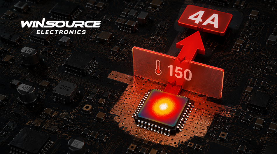
The TLV62595DMQR is a synchronous buck converter that supports an input voltage range of 2.5 V to 5.5 V, an adjustable output voltage from 0.6 V to 4 V, and a maximum output current of 4 A. Its compact package and typical switching frequency of 2.2 MHz make it suitable for high-power-density designs. However, sustained 4 A operation still depends on conversion losses, ambient temperature, PCB thermal performance, external components, and layout conditions. This article examines its practical load-current limits from the perspectives of power loss, thermal design, and component selection.
1. A 4 A Rating Does Not Guarantee Continuous Output Under All Operating Conditions
A buck converter can sustain a given load only when both its electrical and thermal limits are satisfied. The TLV62595 integrates high-side and low-side MOSFETs with typical on-resistances of 26 mΩ and 25 mΩ, respectively. As the load current increases, MOSFET conduction losses rise approximately with the square of the current. Switching losses, inductor losses, and additional losses caused by PCB trace resistance must also be considered. The junction temperature may approach the allowable system limit before the output current reaches the overcurrent-protection threshold.
The relationship between input and output voltage is equally important. For example, when converting 5 V to 1.8 V, the power stage operates at a relatively low duty cycle, with the high-side and low-side switches conducting periodically. When the input voltage approaches the output voltage, the device can enter 100% duty-cycle operation. Under this condition, the available voltage headroom is mainly determined by the high-side MOSFET on-resistance, the inductor DC resistance, and the output current. As the load increases, the resulting voltage drop and heat generation become more significant.
From a system-selection perspective, 4 A is the device’s rated maximum output capability. Whether it can maintain this current continuously must still be verified against the input and output conditions, ambient temperature, and thermal design. Engineering evaluation should define the input-voltage range, output voltage, continuous and peak loads, ambient temperature, and allowable temperature rise. Short-duration full-load operation and continuous full-load operation in a hot, enclosed environment represent different design conditions.
2. Thermal Design in a Compact Package: The PCB Is Critical to Sustained 4 A Operation
The TLV62595DMQR uses a 1.5 mm × 1.5 mm VSON-HR package, making it suitable for high-density power designs. However, its limited package area places greater demands on PCB heat dissipation. At loads approaching 4 A, continuous output capability depends not only on the rated current but also on whether power losses can be transferred effectively through the package pads, copper planes, and PCB layers. Airflow, nearby heat sources, component spacing, and available PCB copper area all affect the actual junction temperature and usable output power.
This means that layout should not be optimized solely for minimum solution size. The input capacitor, output capacitor, and inductor should be placed close to the device. High-current loops should be kept short and provided with sufficient copper width to reduce parasitic inductance, trace voltage drop, and additional heating. The feedback trace should be routed away from the SW node to limit switching-noise coupling into the regulation loop. Excessively reducing copper area, extending high-current paths, or placing the converter near processors, inductors, or other heat sources may result in a significantly higher temperature rise than that observed on the evaluation board.
The TLV62595 includes thermal shutdown at a typical junction temperature of 150°C. This function is intended for abnormal-condition protection rather than normal thermal management. Repeated thermal shutdown not only interrupts the output but also indicates inadequate PCB heat dissipation or insufficient system margin. For applications expected to operate near 4 A for extended periods, copper area, PCB layer structure, and enclosure conditions should be evaluated together with the device specifications.
3. Inductor, Capacitor, and Validation Conditions Determine Whether a 4 A Design Is Viable
The typical TI application uses a 470 nH inductor, a 4.7 µF input capacitor, and either three 10 µF capacitors or one 47 µF output capacitor. These values should be treated as design starting points rather than universal selections. In addition to inductance, the designer should verify peak current, saturation current, and DC resistance. TI recommends selecting an inductor with a saturation-current rating approximately 20% to 30% above the maximum inductor current. Excessive DC resistance increases voltage drop and heat generation, reducing efficiency at high load.
Output-capacitor selection should be based on effective capacitance under DC bias rather than nominal capacitance alone. The TLV62595 requires a minimum effective output capacitance of 20 µF. Insufficient capacitance may increase output ripple and degrade load-transient performance. The input capacitor should also be placed close to the VIN and GND pins to reduce input-current ripple and local voltage drop.
Before the design is finalized, validation should cover the highest and lowest input voltages, maximum continuous load, highest ambient temperature, and worst-case airflow conditions. Measurements should include the temperature near the device, output ripple, and load-transient response. If the system is expected to operate near 4 A for extended periods, additional margin should be reserved for component tolerances, PCB temperature rise, and environmental variation.
The TLV62595DMQR can support a compact 4 A buck-converter design, but its sustained output capability is ultimately determined by system conditions rather than the current rating shown on the first page of the datasheet. For projects requiring verification of TLV62595DMQR package details, lot information, availability, or associated inductor and capacitor selections, WIN SOURCE can provide support during component sourcing and BOM review.
© 2026 Win Source Electronics. All rights reserved. This content is protected by copyright and may not be reproduced, distributed, transmitted, cached or otherwise used, except with the prior written permission of Win Source Electronics.