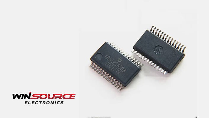
The ADS1256IDBR is a 24-bit high-precision analog-to-digital converter (ADC) developed by Texas Instruments. It uses a delta-sigma (Δ-Σ) modulation architecture, delivering outstanding signal resolution and low noise performance. This chip is widely used in industrial control systems, precision weighing scales, medical signal acquisition, and high-resolution data acquisition platforms. For engineers seeking the highest level of precision, the ADS1256 is more than just an ADC. It serves as the core of a fully programmable analog front-end system.
Architecture Features and Multi-Channel Capability
From an architectural perspective, the ADS1256 adopts a high oversampling Δ-Σ modulator combined with a digital Sinc3 filter. This combination effectively suppresses high-frequency noise. It delivers excellent dynamic range and linearity, making it especially suitable for capturing low-frequency and low-amplitude signals. In practice, it supports sampling rates of up to 30,000 samples per second. It can also be configured to operate at very low sampling rates to maximize noise suppression.
The chip integrates an 8-channel multiplexer for analog input, which can be configured for single-ended or four differential input pairs. This flexibility enhances its suitability for multi-channel measurement systems. In addition, the ADS1256 includes a high-performance programmable gain amplifier (PGA). The PGA supports gain settings from 1 to 64, enabling accurate measurement of microvolt-level signals such as those from strain gauges, thermocouples, and electrochemical sensors.
System-Level Design for High Precision
To truly harness the 24-bit resolution of the ADS1256, careful system-level design is just as important as the chip itself. One critical factor is managing power and reference voltage sources. Although the ADS1256 includes an internal 2.5V reference, using an external precision reference such as the ADR445 or REF5025 is recommended. These options offer improved temperature stability and lower noise, reducing system errors caused by power fluctuations or thermal drift.
On the PCB layout side, it’s essential to separate analog and digital grounds to prevent digital switching noise from interfering with analog signal paths. It’s also recommended to place low-pass RC filters on the analog input lines. These filters help eliminate environmental interference and out-of-band noise. To maintain stable gain and reduce system noise, keep the analog signal traces short, symmetrical, and away from high-frequency digital lines.
Calibration for Long-Term Stability
One of the key strengths of the ADS1256 is its support for multiple calibration mechanisms. It features automatic self-calibration on power-up, and also offers commands for system offset and gain calibration. Engineers can use external shorting or standard voltage sources during these procedures to minimize errors introduced by the signal path. This functionality is particularly important in applications requiring long-term stability, such as laboratory-grade instrumentation or high-end sensor modules.
Additionally, the SPI interface of the ADS1256 is not only stable and highly compatible but also supports communication speeds above 5 MHz. This makes it easy to integrate with various host platforms including MCUs, FPGAs, and single-board computers like Raspberry Pi or BeagleBone.
The Gap Between Theoretical Resolution and Actual ENOB
In real-world applications, the effective number of bits (ENOB) achieved by the ADS1256 is often slightly lower than its theoretical 24-bit maximum. Under well-optimized hardware conditions, it can deliver an ENOB of 21 to 22 bits. However, in systems lacking proper gain configuration, power suppression, or calibration, the ENOB might drop to 17 bits or even lower.
To bridge this gap, engineers need to thoroughly manage all noise sources in the system. It’s important to choose an appropriate combination of sampling rate and PGA gain. Otherwise, there is a risk of overestimating performance based on the nominal specifications. For instance, at a sampling rate of 2.5 samples per second and a PGA gain of 64, the ADS1256 can achieve input noise as low as 0.08μV RMS—ideal for capturing weak signals with high accuracy. However, increasing the sampling rate to 30kSPS improves responsiveness but can also raise the noise level to tens of microvolts or more. Therefore, balancing speed and precision is a critical consideration in any system design using this chip.
Industrial Reliability Meets Development Convenience
The ADS1256IDBR comes in an SSOP-28 package and operates across a temperature range of -40°C to +85°C. It meets industrial-grade reliability standards and benefits from long-term supply stability and strong technical support. These qualities make it a staple in the selection of high-end ADC components.
For development teams, the value of the ADS1256 extends beyond its performance. Its broad compatibility with popular design platforms, mature reference designs, and active community support all contribute to a smoother development process. TI offers official evaluation boards like the ADS1256EVM, and there are numerous open-source drivers available to help speed up prototyping.
The ADS1256IDBR is not a plug-and-play ADC. Instead, it provides a flexible platform that invites deep system optimization. It challenges developers to apply sound analog design practices and thorough noise control strategies. But in doing so, it enables systems to achieve higher resolution, lower error, and greater robustness.
Whether used in medical sensors, industrial weighing systems, precision motion control, or laboratory signal chains, the ADS1256 proves itself as a highly capable 24-bit ADC with exceptional engineering value.
Reliable Sourcing for Precision Projects
In today’s market, where component availability and supply reliability are increasingly crucial, choosing the right ADC is only the first step. Stable procurement and technical support are just as important. As a leading global distributor of electronic components, Win Source not only offers genuine ADS1256IDBR chips in stock but also provides developers with product selection advice, technical documentation, and responsive sourcing channels. This support helps accelerate project delivery and reduce integration risk.
For engineering teams building high-precision data acquisition systems, combining the ADS1256 with Win Source’s dependable supply chain services offers an effective path to achieving the optimal balance of accuracy, efficiency, and cost.
COMMENTS