For two years, the AI chip narrative centered on a single question: can foundries make enough wafers? In 2026, the constraint is gradually extending downstream. The industry can fabricate the silicon — but packaging is where things are getting tight.
TSMC’s CoWoS (Chip-on-Wafer-on-Substrate) capacity, the critical assembly step for many leading AI accelerators, remains sold out through 2026 despite near-tripling output. NVIDIA alone has reserved an estimated 800,000–850,000 wafers of TSMC’s 2026 CoWoS capacity — more than half the total — further compressing available capacity for other customers. The year’s supply-demand gap is estimated at roughly 20%.
The ripple effects are now reaching beyond the packaging houses, into the substrates, thermal solutions, PCBs, and connectors that procurement teams actually buy.
From Silicon Shortage to Packaging Shortage
TSMC has expanded CoWoS capacity from roughly 35,000 wafers per month in late 2024 toward 120,000–130,000 by the end of 2026. It is still not enough. TSMC is expanding its outsourcing cooperation, sending the CoW (Chip-on-Wafer) step to OSAT partners including ASE, Amkor, and SPIL. Previously, TSMC only outsourced the later WoS (Wafer-on-Substrate) stage.
This is a structural change. OSAT-added CoWoS capacity is estimated at 50,000–60,000 wafers per month, with ASE alone targeting 20,000–25,000 wafers per month of its CoWoP variant by year-end. ASE has raised advanced packaging quotes by more than 20%, reflecting higher material costs and capital expenditure.
The message for component buyers: advanced packaging supply continues to tighten, and cost and lead-time pressure is flowing into adjacent materials.
The Component Ripple Effect
ABF substrates — the next bottleneck.
ABF film supply is highly concentrated, with a single Japanese supplier holding more than 95% of global capacity. TSMC’s advanced packaging leadership has warned that ABF substrate shortages could become second only to memory in the years ahead.
On the demand side, AI package layer counts have risen from roughly 12 layers (H100) to 14 (B200/GB300) and toward 18 (Rubin), consuming five to ten times more ABF material than a conventional PC chip. Goldman Sachs projects the ABF supply-demand gap widening from 10% in H2 2026 to 21% in 2027 and 42% in 2028. New substrate capacity takes 2.5–3 years to build, so meaningful relief will not arrive before 2028–2029.
Thermal management — power density is outpacing air cooling.
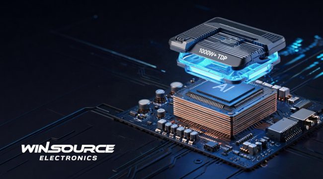
AI accelerators now exceed 1,000W TDP per GPU, with module-level loads reaching 1,200W. High-power designs are driving more projects to evaluate liquid cooling, vapor chambers, and high-conductivity thermal interface materials (TIMs) — and buyers should watch for lead-time and price fluctuation risk across these categories.
High-layer PCBs and connectors.
Few fabricators can handle 30-layer mSAP boards, and those that can are near capacity. High-speed connectors for PCIe 6.0 and CXL 3.0 are also stretching lead times. These are the quiet dependencies of the packaging boom.
What Procurement Teams Should Do Now
- Treat ABF-linked components as critical-path items.Any BOM dependent on high-layer-count substrates, advanced PCBs, or ABF-packaged parts should be reviewed now. Lead times will extend before shortages become visible.
- Qualify thermal solutions early.For AI-adjacent designs, liquid cooling and advanced TIMs may become important options. Lock in qualified suppliers before demand peaks.
- Build second sources for packaging-adjacent passives and connectors.High-speed connectors, power passives, and precision discretes used around advanced packages face growing allocation pressure. Evaluate alternative part numbers, their qualification status, and switching timelines in advance.
- Watch the OSAT expansion wave.ASE, Amkor, and SPIL are ramping capacity and placing equipment and material orders. Their demand for substrates, bonding materials, and test consumables will compete with your own categories.
- Diversify channels for legacy and industrial parts.As suppliers prioritize high-value AI packaging, general-purpose and industrial components risk deprioritization. When OEM or authorized channels are supply-constrained, evaluate qualified independent distribution channels.
Facing the ripple effects of advanced packaging, electronics manufacturers need not only clear strategies but also supply chain execution support. As an independent distributor, WIN SOURCE provides packaging-adjacent components (such as substrates, thermal materials, and high-layer PCBs) through a global supplier network; offers alternative part recommendations validated against DC bias, thermal ratings, and package compatibility; applies IDEA-STD-1010-B visual and anti-counterfeiting inspection standards alongside third-party ISO 17025-accredited laboratory testing to help reduce procurement risk; and provides real-time market intelligence to help procurement teams secure resources before shortages surface.
CoWoS capacity tightening marks a turning point: for some projects, the key constraint is extending from wafers into packaging and materials. For component buyers, the implication is clear — monitor the substrate, thermal, and connector categories now, because the packaging bottleneck may also affect your delivery.
© 2026 Win Source Electronics. All rights reserved. This content is protected by copyright and may not be reproduced, distributed, transmitted, cached or otherwise used, except with the prior written permission of Win Source Electronics.