Computer memory is a vital component of a computer system for storing data and instructions. As one of the physical components of the memory, the memory module (Memory Module) undertakes the tasks of data storage and read and write operations. This article will deeply discuss the structure and working principle of the memory slice, including the physical structure of the memory slice, the organization of the storage unit, the data access process, etc., to help readers better understand the working principle of computer memory.
The physical structure of the memory chip
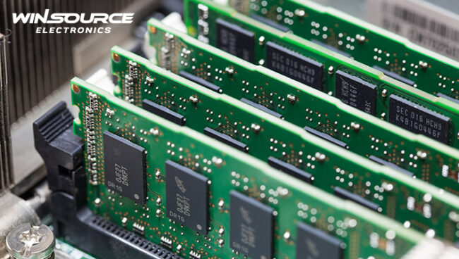
A memory chip is an electronic component that integrates multiple memory chips, usually in the form of a rectangular circuit board. The physical structure of a memory slice includes the following key components:
Memory Chips: Memory chips are the core components of memory chips, responsible for storing and reading data. Common memory chip types include DRAM (Dynamic Random Access Memory) and SRAM (Static Random Access Memory). These chips are connected to the memory chip’s circuit board through a series of circuits and pins.
Pins: Pins are the interface for electrical signal transmission between the memory chip and the computer motherboard. Each memory chip has a certain number of pins, usually made of metal contacts. The number and arrangement of pins depend on the type and specification of the memory chip.
Circuit Board: The circuit board of a memory chip is the basic structure that carries memory chips and pins. It provides the physical support to connect the chip and the motherboard, and realizes the transmission and control of signals through the circuit path.
The organization of the storage unit
The main function of the memory slice is to store data in the storage unit and read it when needed. The storage unit is the smallest data storage unit in the memory chip, which is composed of capacitors or flip-flops in the memory chip. Depending on how they are organized, storage units can be divided into the following two types:
DRAM memory cell: A DRAM memory cell consists of a capacitor and an access line. Capacitors are used to store data, while access lines are used to read and write data. Capacitors in DRAM memory cells need to be periodically refreshed to maintain data correctness. Due to the simple structure of the DRAM storage unit, it can achieve high storage density, but the access speed is relatively slow.
SRAM memory cell: An SRAM memory cell consists of a set of flip-flops, each of which can store a bit (0 or 1). The SRAM storage unit is composed of multiple logic gates, which has high read and write speed and low power consumption. Compared with the DRAM storage unit, the structure of the SRAM storage unit is more complex, so the storage density is relatively low.
Data access process
The data access process of the memory slice includes two stages of data writing and data reading. The following describes how these two stages work:
Data write:
During data writing, the computer transfers the data to be stored to the memory controller. The memory controller is responsible for passing data to the pins of the memory slice. The pins convert the data signal into an electrical signal and transmit it through the circuit board into the memory chip. The memory chip writes the received data into the corresponding storage unit, and sends an acknowledgment signal after the writing is completed.
Data read:
During data reading, the computer sends a read request to the memory controller. The memory controller determines where the required data is stored and passes read requests to the pins of the memory slice. The pins convert the read requests into electrical signals that are transmitted across the board and into the memory chip. The memory chip reads data from the corresponding storage unit according to the read request, and passes the data to the memory controller through the pin, and finally passes the data to the computer for processing.
It is worth noting that the data access speed of a memory chip is affected by many factors, including the type of memory chip, memory frequency, and data bus width. Higher memory frequencies and wider data buses can increase data transfer speeds, thereby improving the overall performance of a computer system.
Application of memory chips
As an important component in computer systems, memory chips are widely used in various fields, including personal computers, servers, and embedded systems. Different application scenarios have different requirements for memory slices. For example, personal computers usually require higher storage capacity and speed, while servers pay more attention to stability and reliability.
In addition, the memory chip can also expand the total memory capacity of the system by increasing the number of modules. This expansion provides more storage space and enables the computer to handle more data and tasks at the same time.
In conclusion, a deep understanding of how memory slices are constructed and how they work helps us better understand how computer memory works. Memory slices play an important role in computer systems, and their selection and application are critical to computer performance and system stability. With the continuous development of technology, memory chips will continue to improve and innovate, providing computer systems with more powerful storage and processing capabilities.
COMMENTS