Overview
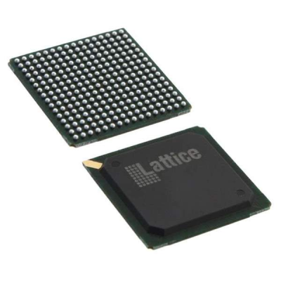
low-power, cost-effective FPGA (field programmable gate array) launched by Lattice Semiconductor , belonging to the ECP2M series . With its excellent performance and versatility, this device is widely used in industrial automation, communication infrastructure, consumer electronics and embedded systems . LFE2M20E-5FN256C provides up to 20,000 logic units (LUTs) , integrates high-speed SERDES channels, DSP blocks and rich I/O interfaces, which can meet complex data processing requirements and achieve low-power design.

Specifications
parameter | Numeric |
Logic Unit (LUT) | 20,000 |
Embedded storage (RAM) | 414 Kbits |
Number of DSP blocks | twenty four |
Clock management unit (PLL) | 4 |
High-speed SERDES channels | support |
Maximum number of user I/O pins | 195 |
Package Type | 256-pin FBG (Fine Pitch BGA) |
Operating voltage range | 1.2V core voltage, 3.3VI/O voltage |
Power Optimization | Dynamic power management, low power design |
Operating temperature range | -40°C to +85°C (Industrial) |
Key features of LFE2M20E-5FN256C
High-density logic resources to support complex designs
It provides 20,000 logic units (LUTs) and rich embedded storage resources, providing users with sufficient hardware foundation to implement complex FPGA designs.
It is suitable for application scenarios such as signal processing, data communication, protocol bridging, control logic and state machine implementation .
Integrated DSP blocks to accelerate signal processing
The device contains 24 DSP blocks , which provide hardware acceleration for mathematical operations such as filtering, signal modulation, FFT, and image processing to improve computing efficiency.
High-speed SERDES channel to enhance data transmission capability
Supports SERDES (Serial Deserializer) communication interface for high-speed data transmission, suitable for applications such as Gigabit Ethernet, fiber optic communication and PCI Express .
Multiple I/O interfaces to enhance system flexibility
The LFE2M20E-5FN256C has 195 user I/O pins and supports multiple I/O standards such as LVCMOS, LVDS, and SSTL , providing greater flexibility for system design.
Supports DDR2, SPI, I²C and other common peripheral interfaces to enhance device compatibility.
Low power consumption design to extend system life
Lattice’s low-power architecture uses dynamic power management mechanisms to reduce FPGA operating energy consumption, making it particularly suitable for portable devices, IoT nodes and other applications that require high energy efficiency .
Flexible packaging and industrial temperature support
The 256-pin FBG (Fine Pitch BGA) package provides greater PCB design flexibility while maintaining high-density logic resources.
Industrial temperature range (-40°C to +85°C) ensures stable and reliable performance in industrial control and harsh environments.
Application Areas
high-efficiency and low-power FPGA , LFE2M20E-5FN256C is widely used in the following fields:
Industrial Automation and Control
Programmable logic controller (PLC), industrial robot, motion control system
Provides reliable logic implementation, fast response and protocol bridging capabilities to improve the flexibility and stability of automation systems.
Communications and Network Equipment
Network switches, Gigabit Ethernet devices, fiber optic communication modules
Supports high-speed SERDES interface and multiple I/O standards, providing efficient hardware support for data communication and protocol conversion.
Consumer electronics and multimedia processing
High-definition video processing, audio signal processing, image enhancement equipment
With the help of DSP blocks, complex audio and video signal processing is realized to enhance the user’s multimedia experience.
Internet of Things and Embedded Systems
Smart home gateways, IoT nodes, edge computing devices
Low power consumption and flexible I/O support help IoT devices achieve efficient connection and data processing.
Military and avionics
Data encryption module, radar signal processing, flight control system
Industrial-grade temperature range and high reliability ensure stable operation of the equipment in harsh environments.
Advantages of LFE2M20E-5FN256C
Features/Specifications | LFE2M20E-5FN256C | Competing FPGA Products |
Number of logic units (LUT) | 20,000 | 15,000 – 18,000 |
Number of DSP blocks | twenty four | Some products do not support DSP acceleration |
High-speed SERDES support | yes | Some low-end FPGAs do not support |
User I/O pin count | 195 | 100 – 160 |
Power Optimization | Dynamic power management, low power design | No dedicated power optimization mechanism |
Temperature range | -40°C to +85°C | -40°C to +70°C |
Compared with other low-end FPGA products, LFE2M20E-5FN256C performs better in terms of logic resources, DSP acceleration, high-speed data transmission capabilities, industrial-grade temperature support, etc., making it an ideal choice for complex application scenarios.
Manufacturer introduction: Lattice Semiconductor
Lattice Semiconductor is a leading global provider of low-power FPGA solutions, dedicated to providing efficient and flexible FPGA products for the industrial, communications, consumer electronics and automotive markets. LFE2M20E-5FN256C is a representative model of its ECP2M series products with high performance and low power consumption, and is widely used in the global market.
Why choose LFE2M20E-5FN256C?
● 20,000 logic cells to support complex designs
● 24 DSP blocks to improve signal processing efficiency
● High-speed SERDES interface, supporting Gigabit Ethernet and fiber optic
● communications 195 user I/Os, supporting multiple communication standards and peripheral
● interfaces Industrial temperature range (-40°C to +85°C) for harsh
● environments Low power consumption design, extending battery life and reducing system energy consumption
● Compact FBG package improves PCB layout flexibility
LFE2M20E-5FN256C is a high-performance, high-efficiency, low-power multi-function FPGA suitable for a variety of application scenarios such as industrial automation, communication infrastructure, embedded systems and consumer electronics , providing a powerful and flexible solution for embedded design.
FAQ
Q1: Does LFE2M20E-5FN256C support Gigabit Ethernet applications?
A: Yes, LFE2M20E-5FN256C supports high-speed SERDES interface, suitable for Gigabit Ethernet and other high-speed communication protocols.
Q2: How is the power consumption of this device?
A: LFE2M20E-5FN256C adopts Lattice’s low power architecture and effectively reduces operating energy consumption through dynamic power management mechanism, which is suitable for IoT devices and battery-powered devices.
For more details and to explore our inventory, please visit the links below:
Product Details: Win Source – LFE2M20E-5FN256C
©2025 Win Source Electronics. All rights reserved. This content is protected by copyright and may not be reproduced, distributed, transmitted, cached or otherwise used, except with the prior written permission of Win Source Electronics.

COMMENTS