Overview
XC7K70T-1FBG484C is a medium-capacity model in the Kintex-7 series FPGA launched by AMD (formerly Xilinx), designed to provide high-performance and low-power solutions in high-speed communications, signal processing, industrial control, image recognition and embedded platforms. The chip is manufactured based on a 28nm low-power process, integrating a large number of programmable logic units, DSP resources, Block RAM and high-speed serial transceivers (GTX), and uses a 484-pin FBG484 BGA package, which is suitable for application systems with high requirements for bandwidth, logic density and power consumption.
Specifications
parameter | Numeric |
Device Series | Kintex-7 |
Logic Units (LUTs) | 65,600 |
Logical registers (FFs) | 102,400 |
Block RAM Capacity | 4,860 KB (60 blocks of 36Kb) |
Number of DSP multipliers | 240 (18×25) |
GTX High-Speed Transceivers | 4 channels, up to 6.6Gbps |
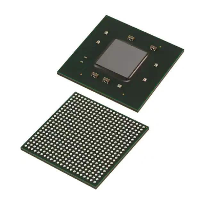
Package Type | FBG484 (484-pin BGA, 1.0mm pitch) |
Package size | 23mm x 23mm |
Speed Rating | -1 (standard speed grade) |
Operating temperature range | 0°C to +85°C (commercial grade, C) |
Number of I/O pins | Up to 240 user I/Os |
Supply voltage range | Core voltage 1.0V, I/O supports 1.2V–3.3V |
XC7K70T-1FBG484C Core Features
Perfect balance of high performance and medium logic density
With 65K+ logic cells and 100K+ registers, it is suitable for implementing medium-complexity control, operation, and interface logic, achieving an ideal balance between performance and power consumption.
Built-in 4-channel GTX transceiver
It supports serial transmission rates of up to 6.6Gbps per channel and can implement high-speed interface protocols such as PCIe Gen2, Aurora, SATA, and Serial RapidIO.
Rich DSP and storage resources
It has 240 built-in DSP48E1 units and approximately 4.8Mb of Block RAM, supporting high-speed numerical calculations and large-scale buffering, image caching and filtering algorithms.
Low power consumption 28nm process, excellent thermal performance
Power consumption is reduced by up to 50% compared to previous generation FPGAs, making it suitable for battery-powered, thermally constrained systems.
High pin density BGA package, suitable for various PCB designs
The FBG484 package provides sufficient I/O and differential pair counts while occupying a small board space, facilitating high-density board layout.
Compatible with Vivado Design Suite and rich IP resources
Supports Xilinx Vivado platform for design, simulation and deployment, and is equipped with a variety of Xilinx IP Cores, logic analysis tools, and soft-core processors (MicroBlaze) to improve development efficiency.
Typical application scenarios
With its excellent computing power, IO flexibility and high-speed interface support, XC7K70T-1FBG484C is widely used in:
5G and Wired Communication Systems
Used as MAC layer processor, high-speed interface bridge, protocol encapsulation and decapsulation, data channel scheduling, etc.
Industrial Automation and Motor Control
Realize high-precision PWM control, current detection and feedback, and real-time controller functions to replace MCU/DSP.
Image Processing and Edge Computing
Used for camera interface bridging, image filtering, feature extraction, real-time preprocessing and other medium and high complexity image algorithms.
Medical electronics and wearable devices
Integrates data acquisition, digital filtering and system control to meet the needs of low power consumption and high integration.
Aerospace and Military Electronic Systems
The data processing system meets the requirements of anti-interference, low latency and high security, which facilitates the implementation of customized logic.
Advantages comparison analysis
Comparison Items | XC7K70T-1FBG484C | Spartan-6 (such as XC6SLX75) |
Process Node | 28nm | 45nm |
GTX Transceivers | Yes, 4 channels | none |
Power consumption performance ratio | Lower power consumption, improved performance | High power consumption |
Support interface protocol | PCIe, SATA, Aurora, etc. | SPI, UART, low-speed interface |
RAM and DSP quantity | Bigger | Less than half of XC7K70T |
Vivado Support | yes | Need to use the old version of ISE |
XC7K70T provides stronger performance, richer resources and more advanced development support than the Spartan series, and is suitable for project upgrades with higher requirements for system performance.
Manufacturer Profile: AMD / Xilinx
Xilinx (now a brand of AMD) is the world’s leading provider of FPGA and programmable logic solutions. The Kintex-7 series is a representative product of mid-range performance and is widely deployed in communications, data centers, industrial and defense electronic systems. As the backbone model of the series, XC7K70T-1FBG484C provides excellent performance-to-density ratio and extremely high reliability.
Why choose XC7K70T-1FBG484C?
65K+ LUTs and 240 DSPs to meet medium-complexity system design
● Built-in 4-channel GTX transceiver , supporting mainstream high-speed interface protocols
● 28nm process and low-power architecture , suitable for portable and heat-sensitive devices
● Support Vivado + rich IP Core , high design efficiency and short cycle
● Medium package size (FBG484) , rich I/O, adapt to high-speed design requirements
● Wide industry adaptability , covering communications, industry, image processing, etc.
FAQ
Q1: Can XC7K70T run PCIe interface?
Yes, XC7K70T supports running PCI Express interface. This FPGA integrates multi-channel GTX high-speed serial transceivers, which can realize the physical layer transmission of PCIe Gen1 and Gen2, and supports x1, x2 and x4 channel configurations. Users can call the PCIe Block IP provided by Xilinx in Vivado Design Suite to implement a complete PCIe protocol stack, including PHY, DLL and TLP layers, to simplify the design process. It also supports user-defined protocol layer logic, which is suitable for embedded systems, high-speed communications or data acquisition applications that require more flexible customization.
Q2: What development tools does this model support?
It supports Vivado Design Suite (version 2020.1 and above is recommended), and can use IP Integrator, Timing Analyzer, and Power Estimator tools.
For more details and to explore our inventory, please visit the links below:
Product Details: Win Source – XC7K70T-1FBG484C
©2025 Win Source Electronics. All rights reserved. This content is protected by copyright and may not be reproduced, distributed, transmitted, cached or otherwise used, except with the prior written permission of Win Source Electronics.
COMMENTS