* Question
How do I configure the FPGA using Boundary Scan mode (JTAG mode)?
* Answer
Here’s a clear, vendor-neutral checklist you can follow to configure an FPGA via Boundary-Scan (JTAG) mode. It covers both volatile (SRAM) download and indirect programming of config flash.
Table of Contents
ToggleWhat you need
Bitstream / programming file from your toolflow
AMD/Xilinx: .bit (SRAM), .mcs/.bin (config flash via indirect)
Intel/Altera: .sof (SRAM), .jic/.pof (flash)
Lattice/Microchip: device-specific (e.g., .bit/.svf for SRAM; .jed/.bin or vendor flash image for NVM)
For 3rd-party JTAG players: SVF/XSVF/JAM files
JTAG cable (Platform Cable/HSx, USB-Blaster, FlashPro, Lattice Cable, etc.)
Powered target board with accessible TCK, TMS, TDI, TDO, GND (and Vref if your cable uses it)
Board & wiring checks (before you start)
Power rails up and stable (core, I/O banks; level shifters powered).
Boot-mode straps (MSEL / M[2:0] / CFGx) set appropriately. (JTAG usually works regardless, but set to JTAG/“no auto boot” if you want to prevent other modes.)
JTAG chain integrity: correct daisy-chain order, short cables, solid ground, no TDO pull-downs.
Start with a conservative TCK (e.g., 1–6 MHz) if the chain is long or goes through level shifters.
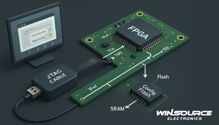
A) Volatile configuration (load design to SRAM over JTAG)
Open the vendor programmer
AMD/Xilinx: Vivado Hardware Manager → Open Target → Program Device
Intel: Quartus Programmer → Auto Detect → Add File (.sof)
Lattice: Diamond Programmer → Scan Chain → SRAM Program (.bit/.svf)
Microchip: Libero/FlashPro → Scan Chain → Program
Detect the chain and verify the FPGA IDCODE matches the part.
Assign the bitstream to the FPGA device in the chain.
(Optional) Set options like verify after programming, readback, keep device in JTAG state.
Program. Watch status pins (e.g., DONE/INIT_B or CONF_DONE) and the tool’s log for success.
If the device immediately “forgets” the design after reset/power-cycle, that’s expected—SRAM configuration is volatile. Use section B to make it persistent.
B) Indirectly program the configuration flash via JTAG (persistent boot)
Convert your design to a flash image in the vendor tool
AMD/Xilinx: Generate Memory Configuration File → .mcs/.bin (select the right SPI/QSPI part)
Intel: Convert Programming Files → .jic/.pof
Others: make the vendor-specific flash image or SVF/JAM for your board’s flash
In the programmer, choose Add Configuration Memory Device (or equivalent), select the exact flash model on your board.
Program + Verify the flash over JTAG.
Power-cycle or toggle PROGRAM_n to let the FPGA boot from flash. Confirm DONE/CONF_DONE = High and the design runs at reset.
Using SVF/XSVF/JAM with 3rd-party JTAG
If you aren’t using vendor GUIs, export an SVF/XSVF/JAM from the tool and play it with your JTAG controller (OpenOCD, UrJTAG, etc.).
Ensure you include verify steps in the script and set a reasonable TCK.
Common pitfalls & quick fixes
Chain not detected / IDCODE wrong → check TDO continuity, reduce TCK, ensure Vref/level shifters powered, remove other devices from reset.
Programming fails at verify → slow TCK, shorten cable, add ground strap, check flash part selection.
DONE/CONF_DONE low after power-cycle → wrong flash density/model, missing boot-mode straps, corrupt image, or the flash not actually programmed.
No JTAG access → device security set (bitstream encryption / JTAG disable); clear per vendor procedure.
Autoboot interfering → hold PROGRAM_n/INIT low (Xilinx) or nCONFIG low (Intel) during setup, or strap for JTAG mode during bring-up.
Minimal “recipe” you can paste into a lab sheet
Power board → connect JTAG (TCK/TMS/TDI/TDO/GND).
Launch programmer → Auto-detect chain (verify IDCODE).
SRAM load: add .bit/.sof → Program → check DONE.
Make persistent: convert to flash image (.mcs/.jic/…) → add configuration memory → Program + Verify → Power-cycle → check DONE.
Document tool version, device ID, flash part, TCK, success logs for traceability.
COMMENTS