*Image from the internet; all rights belong to the original author, for reference only.
Inside onsemi EPP: A Wafer-Level Approach to Power Integration
Quick Take
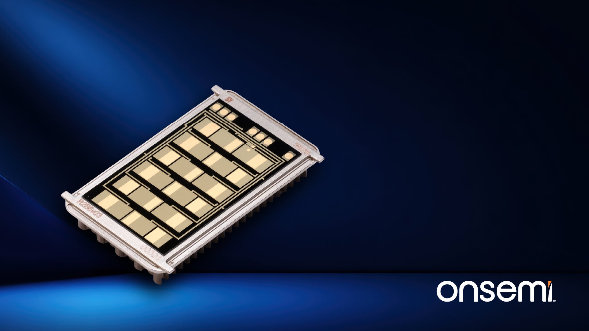
- onsemi’s Embedded Power Platform embeds silicon, SiC or GaN dies into a silicon-based package and connects them through wafer-level redistribution layers.
- Replacing traditional wire bonds with shorter, controlled interconnects is intended to reduce parasitic inductance and improve switching and thermal performance.
- EPP can integrate FETs, drivers, controllers and high-voltage isolation, but external capacitors, magnetics, sensors, connectors and cooling hardware remain part of the complete system.
- The platform is expected to begin sampling with selected automotive and AI customers in 2026.
Background
On September 16, 2026, onsemi introduced the Embedded Power Platform, or EPP, for automotive, industrial and AI power applications.
The important feature is not simply that EPP combines several components. It changes how power dies are packaged and interconnected. Heterogeneous semiconductor dies are embedded in a silicon structure and connected through wafer-level metallization rather than relying only on conventional substrates and wire bonds.
This makes EPP a packaging and power-integration development rather than another individual MOSFET launch. Its potential value depends on whether the architecture can deliver lower electrical parasitics, better heat flow and greater power density in commercial products.
Q1. What does “using the silicon wafer as the package” mean?
Conventional power packaging typically attaches semiconductor dies to a substrate and then uses wire bonds, clips or other conductors to connect them to the package terminals. The semiconductor and its package are manufactured as distinct elements before being assembled.
EPP moves key integration steps into a wafer-level process. Power and control dies are embedded in a silicon-based structure, while precisely patterned redistribution layers provide the electrical connections. The silicon structure therefore contributes to the interconnection, isolation, mechanical construction and thermal path instead of serving only as passive housing.
The platform is designed to accommodate different die technologies, including silicon, SiC MOSFETs and GaN FETs. Gate drivers, controllers and other semiconductor functions can also be embedded in configurable combinations.
Q2. How is EPP different from a conventional power module?
Both EPP and conventional power modules can combine multiple dies in one assembly. The main difference lies in the integration method.
Traditional modules commonly use an insulated substrate, die-attach materials, wire bonds or metal clips, and a separate baseplate or housing. EPP shifts more of this construction into a silicon-based wafer process. Its redistribution layers replace traditional wire-bond connections, while high-voltage isolation can be incorporated into the package.
EPP should therefore not be described simply as “more integrated.” Its distinctive feature is that semiconductor fabrication methods are being applied to the package and interconnect structure.
However, the practical comparison will ultimately depend on specific products. EPP datasheets will need to show voltage and current ratings, isolation capability, thermal resistance, switching performance, mechanical durability and reliability before engineers can compare it with existing power modules.
Q3. Why do shorter interconnections matter in a power system?
Every conductor has some parasitic resistance and inductance. In fast-switching power circuits, the inductance of wire bonds, package leads and PCB traces can produce voltage overshoot, ringing, electromagnetic interference and additional switching losses.
This becomes particularly important with SiC and GaN devices because their fast switching edges can expose limitations in the surrounding interconnects. A high-performance transistor cannot deliver its full system-level benefit if package parasitics restrict switching speed or require conservative operating conditions.
EPP uses shorter, more controlled redistribution layers to connect the embedded dies. According to onsemi, this reduces parasitic inductance, improves device control and supports higher switching frequencies.
The architecture also allows power devices and their gate drivers to be placed in closer electrical proximity. That can reduce the length of critical gate-drive loops, although the exact benefit will depend on the configuration of each future EPP product.
Q4. How does the silicon-based structure affect heat dissipation?
Power density is limited not only by transistor efficiency but also by how effectively heat can leave the package. Conventional modules may contain several material interfaces between the die, insulating layer, substrate, baseplate and cooling system. Each interface contributes to the overall thermal path.
onsemi says EPP uses the silicon-based structure and more of the package footprint to conduct heat. The platform also integrates high-voltage isolation, reducing reliance on some insulating materials that may impede heat flow.
In an early EPP-based solid-state circuit-breaker design for AI infrastructure, onsemi reports that the solution was approximately 50% smaller and operated about 20% cooler than the compared design. For EV traction inverters, the company reports up to four times higher power density and 15% lower power losses.
These are early design results rather than universal specifications. Cooling method, switching topology, semiconductor selection and operating conditions will determine the performance of individual implementations.
Q5. Which components can EPP integrate—and which remain external?
EPP can embed combinations of power FETs, gate drivers, controllers and high-voltage isolation. Depending on the final design, this could remove some separate packages, wire-bond connections and board-level driver interconnects.
It does not turn an inverter, circuit breaker or power converter into a single self-contained component. A complete system may still require:
- DC-link and decoupling capacitors;
- inductors, transformers or other magnetic components;
- current, voltage and temperature sensors;
- EMI filtering and surge-protection components;
- connectors, busbars and cable assemblies;
- auxiliary power supplies;
- control processors and communication interfaces;
- heatsinks, cold plates or other cooling hardware.
Whether an isolation function, sensor or controller remains external will depend on the boundary of the particular EPP implementation. Engineers should therefore evaluate the complete block diagram rather than assume that every supporting function has moved inside the package.
For component sourcing, the immediate opportunity remains broader than EPP itself. Higher-density power systems still require capacitors, magnetics, sensing, protection, connection and thermal-management components matched to the new electrical and thermal conditions.
Q6. What should engineers watch as EPP moves toward sampling?
onsemi expects EPP sampling to begin in 2026 with selected automotive and AI customers and ecosystem participants. Subaru is receiving early access to engineering samples, simulation models and technical expertise to evaluate the platform for future electrified vehicles. This is an engineering evaluation, not a confirmed production selection.
The next decisive information will be product-level rather than architectural:
- orderable part numbers and datasheets;
- available die combinations and package formats;
- voltage, current and isolation ratings;
- switching and short-circuit behavior;
- thermal resistance and cooling requirements;
- reliability and automotive qualification results;
- reference designs, simulation models and evaluation hardware;
- general production and availability schedules.
Until these details are published, EPP is best understood as a new integration architecture. It does not yet provide a direct, orderable replacement for existing discrete SiC MOSFETs, GaN FETs or conventional power modules.
Conclusion
onsemi EPP is technically significant because it brings power dies, control functions, interconnects, isolation and heat flow into a silicon-based wafer-level structure. Its most important innovation is not simply putting more components in one package, but using semiconductor-style fabrication to improve the package itself.
The early AI circuit-breaker and EV inverter results indicate where this approach could be useful: applications constrained by switching parasitics, cooling capacity, weight and available space. The next step is to translate the architecture into documented and qualified products. Datasheets, package configurations, reliability results and engineering samples will show how EPP compares with established power modules in practical designs.
© 2026 Win Source Electronics. All rights reserved. This content is protected by copyright and may not be reproduced, distributed, transmitted, cached or otherwise used, except with the prior written permission of Win Source Electronics.