* Question
What are the reasons for the zero residual voltage?
* Answer
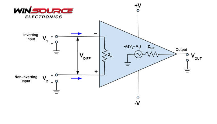
Zero residual voltage refers to a situation where the voltage difference between the inverting and non-inverting inputs of an operational amplifier (op-amp) is zero or negligible, resulting in no detectable offset between the two inputs. Achieving zero residual voltage is important for high-precision applications, where even small voltage differences can lead to significant errors.
There are several key reasons or conditions that can contribute to zero residual voltage in an op-amp or circuit:
1. Perfect Matching of Input Transistors (Input Differential Pair)
– In an ideal op-amp, the transistors in the input differential pair (the pair of transistors that receive the input signal) are perfectly matched, meaning that they have identical electrical characteristics. This ensures that the voltage difference between the inputs is zero when the output is at the correct level.
– Matched transistors ensure minimal imbalance and therefore minimal residual voltage. In real-world op-amps, however, there will always be some minor mismatch, but it can be minimized through careful design and selection of components.
2. Low Input Offset Voltage
– Input offset voltage is the small voltage difference that exists between the inverting and non-inverting inputs, even when the output should ideally be zero. In high-precision op-amps, the input offset voltage can be minimized through design techniques, such as laser trimming of the input transistors or auto-zeroing.
– When the input offset voltage is extremely low (or zero), the residual voltage between the input terminals can be negligible or effectively zero.
3. Negative Feedback
– Negative feedback plays a crucial role in maintaining zero residual voltage by adjusting the op-amp’s output to ensure the voltage difference between the inputs is as small as possible.
– In a properly designed closed-loop configuration, the op-amp works to equalize the voltage at both inputs by driving the output to compensate for any difference. When the loop is properly closed and the op-amp is operating within its linear region, it can drive the voltage difference between the inputs close to zero.
4. Zeroing Techniques
– Some high-precision systems use auto-zeroing or servo systems to actively measure and correct the input offset voltage over time. This method adjusts the op-amp’s internal circuitry to cancel any offset voltages, effectively driving the residual voltage to zero.
– External trimming can also be applied to manually adjust the op-amp’s internal circuitry to compensate for any residual offset voltage.
5. Use of High-Precision Op-Amps
– Some precision op-amps are specifically designed to minimize residual voltage. These op-amps feature very low input offset voltage and low drift characteristics, which help maintain zero residual voltage over temperature variations, supply voltage changes, and over time.
6. Proper Circuit Design (Balanced Inputs)
– Ensuring that the circuit design has balanced inputs and equal impedance for both the inverting and non-inverting inputs can reduce the likelihood of creating unwanted voltage differences between the inputs. A balanced design minimizes the risk of inducing an unwanted residual voltage due to asymmetry in the input stage.
7. Environmental Factors and Temperature Compensation
– Temperature variation can lead to changes in the characteristics of the transistors and other components, which might increase the input offset voltage. Precision op-amps often incorporate temperature compensation mechanisms to reduce the effect of temperature changes on the residual voltage.
– In some designs, external compensation circuits are used to track temperature changes and adjust the op-amp’s performance accordingly.
8. Low-Noise Circuit Design
– Noise can sometimes contribute to residual voltage due to the inherent electrical noise in the components (e.g., thermal noise, flicker noise). By using low-noise components and minimizing interference from external sources, the residual voltage can be kept very low.
– Proper grounding, shielding, and layout techniques can help reduce noise-induced voltage differences.
Summary of Reasons for Zero Residual Voltage:
1. Perfect matching of input transistors (ensuring no mismatch between the differential pair).
2. Low input offset voltage (minimizing any intrinsic offset that would cause a voltage difference between inputs).
3. Negative feedback (actively minimizing input voltage differences in closed-loop operation).
4. Zeroing techniques (auto-zeroing or trimming systems to adjust and eliminate any residual voltage).
5. Use of high-precision op-amps (devices specifically designed for low offset and high accuracy).
6. Balanced circuit design (ensuring equal impedance and symmetry between the input paths).
7. Temperature compensation (minimizing the effect of environmental changes on offset voltage).
8. Low-noise design (reducing noise that could contribute to voltage differences between inputs).
By implementing these techniques, the op-amp or circuit can maintain minimal or zero residual voltage, ensuring high precision in applications like instrumentation, signal conditioning, and high-fidelity audio systems.
COMMENTS