* Question
What is the internal photoelectric effect in semiconductors?
* Answer
The internal photoelectric effect refers to the phenomenon in which light energy absorbed by a material excites charge carriers (electrons and holes) within that material, thereby changing its electrical conductivity.
Unlike the external photoelectric effect, where electrons escape from the material’s surface, the internal effect occurs inside the solid—most commonly in semiconductors and photoconductive materials.
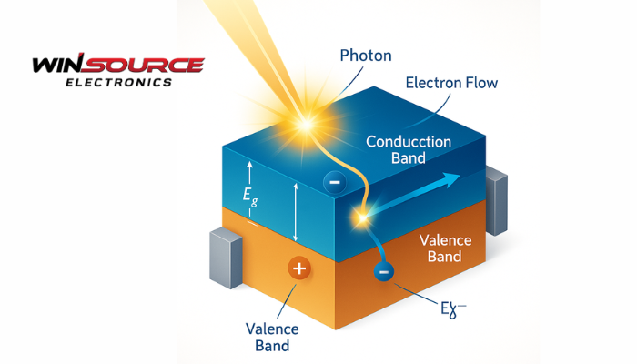
1. Fundamental Mechanism
When photons with sufficient energy strike a semiconductor, their energy is absorbed by electrons in the valence band.
If the photon energy exceeds the band gap (Eg) of the material, these electrons gain enough energy to jump into the conduction band, leaving behind holes in the valence band.
This process generates electron–hole pairs, which can move under an electric field, producing a measurable photocurrent.
Mathematically, the condition for excitation is:
hν≥Eg
where hν is the photon energy and Eg is the semiconductor band gap.
2. Key Characteristics
- Occurs inside the material:Electrons remain within the solid rather than being emitted from it.
- Increases conductivity:The creation of electron–hole pairs enhances charge transport.
- Depends on photon energy:Only light with energy equal to or greater than the band gap can trigger the effect.
- Reversible and repeatable:Once illumination stops, recombination occurs and the material returns to its initial state.
3. Typical Applications
The internal photoelectric effect is the fundamental principle behind most optoelectronic devices, including:
- Photodiodes– convert light into electrical current.
- Phototransistors– amplify the photo-generated signal.
- Solar cells– generate electric power from sunlight.
- CCD/CMOS sensors– detect light intensity in imaging systems.
Each of these devices uses specific semiconductor structures to optimize photon absorption, carrier separation, and current extraction.
4. Difference from External Photoelectric Effect
Feature | Internal Photoelectric Effect | External Photoelectric Effect |
Electron Behavior | Electrons excited within material | Electrons ejected from surface |
Material Type | Semiconductors, photoconductors | Metals or photoemissive materials |
Result | Increased conductivity or photocurrent | Emission of electrons into vacuum |
Applications | Solar cells, photodiodes | Photoelectron tubes, vacuum sensors |
Summary Insight
In essence, the internal photoelectric effect is the foundation of modern optoelectronics, enabling light-to-electric conversion inside semiconductors.
It underpins critical technologies—from solar energy harvesting to optical sensing and digital imaging—by leveraging the quantum interaction between photons and electronic band structures.
COMMENTS