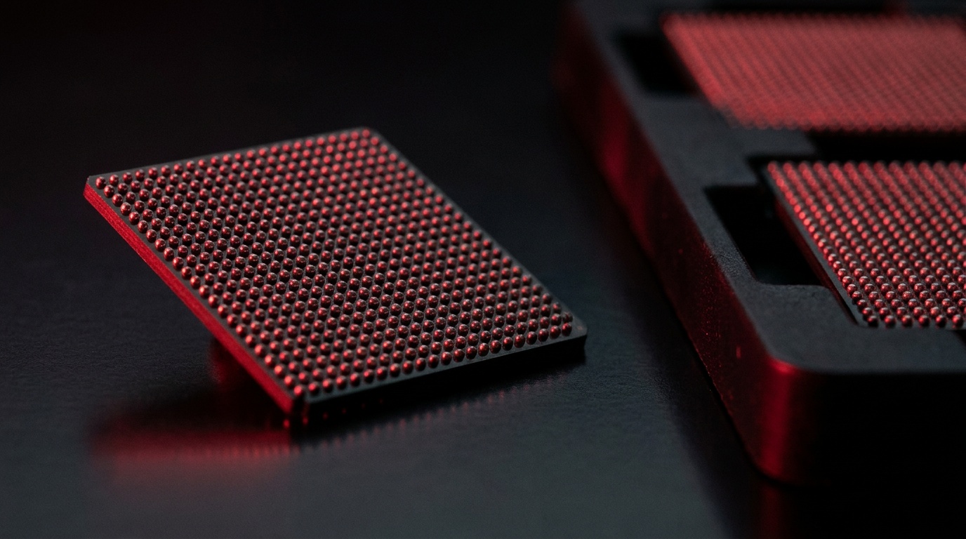
A Field-Programmable Gate Array, or FPGA, is one of the more unusual components in modern electronics: it is a chip that ships blank and gets its logic written in after the fact — by the engineer, not the manufacturer. That single property — the ability to define hardware behavior in software and reprogram it as requirements change — is what has made FPGAs indispensable in applications ranging from 5G base stations and aerospace systems to machine learning accelerators and industrial control.
This article covers the fundamentals of FPGA architecture, explains the internal building blocks that make reprogrammability possible, surveys the major vendors and their product families, and addresses a topic that rarely gets enough attention in introductory guides: what happens when the FPGA your design depends on reaches end-of-life, and how engineering and procurement teams can navigate that situation.
What Is an FPGA?
An FPGA is an integrated circuit that contains a large array of programmable logic elements connected by a configurable routing network. Unlike a microprocessor, which executes instructions sequentially in software, an FPGA implements logic directly in hardware — the physical connections between logic cells are set by a configuration file loaded at power-up or stored in on-chip flash memory. This means that many operations can run in parallel rather than in sequence, which gives FPGAs a performance and latency profile that general-purpose processors simply cannot match for certain workloads.
The term “field-programmable” refers to the fact that the device can be programmed outside of the factory — in the field, by the end user. This distinguishes FPGAs from Application-Specific Integrated Circuits (ASICs), which are designed for one fixed function and cannot be changed after fabrication. The tradeoff is that FPGAs consume more power per operation than equivalent ASICs and cost more per unit at volume, but they do not require the nonrecurring engineering (NRE) investment, mask set and design cycle an ASIC demands. For prototyping, low-to-medium volumes, or applications where the algorithm may change over time, FPGAs often make more sense.
FPGA Architecture: How the Pieces Fit Together
Understanding how an FPGA works at a structural level helps clarify both its strengths and its limitations. The core of any FPGA is built from three fundamental components: an array of configurable logic blocks, a programmable interconnect network, and programmable I/O blocks at the chip’s periphery. Modern devices also include hardened (non-programmable) silicon blocks for functions like digital signal processing and high-speed serial transceivers.
Configurable Logic Blocks (CLBs) and Look-Up Tables
The fundamental unit of logic in most FPGAs is the Configurable Logic Block (CLB). In the Xilinx-family devices now sold by AMD, for example, the CLB is the primary logic element, each one built around one or more look-up tables (LUTs) and flip-flops. A Look-Up Table (LUT) is essentially a small piece of SRAM that stores a truth table: given a set of binary inputs, the LUT outputs a pre-programmed result. A basic logic element consists of a LUT and a flip-flop; a LUT with k inputs holds 2k configuration bits and can implement any k-input Boolean function. Most modern FPGAs use 6-input LUTs (LUT-6), which can represent any function of six variables and offer a good balance between logic density and routing efficiency.
A CLB typically contains a cluster of these basic logic elements connected through a local routing network, allowing logic that communicates frequently to be placed physically close together, which reduces delay. The configuration data for all LUTs and routing switches is held in static RAM cells across the chip; loading a new bitstream into those SRAM cells changes the chip’s entire logical behavior, which is how reconfiguration works.
Programmable Interconnect
The interconnect fabric is responsible for routing signals between CLBs, and its quality has an outsized effect on performance. The central array of logic blocks is connected through a configurable interconnect routing matrix built from programmable switch boxes and wire segments of varying lengths. Most designs exhibit locality and therefore need abundant short wires, but they also contain distant connections that call for sparser long wires, so the routing architecture has to serve both without wasting area.
The routing architecture is one area where vendors differentiate significantly. Too little routing flexibility and the designer cannot fit a complex design onto the chip; too much, and the overhead in area and power becomes unacceptable. Getting this balance right is one of the core engineering challenges in FPGA architecture design, and it is a major reason why synthesis and place-and-route tools are critical to the design flow.
I/O Blocks
Around the periphery of the logic array sits a ring of I/O blocks that can be configured to support different interface standards. These I/O blocks handle the electrical interface between the FPGA’s internal logic and the outside world — setting drive strength, slew rate, pull-up/pull-down resistors, and support for standards such as LVDS, LVCMOS, and SSTL. On high-end devices, the I/O periphery also includes high-speed serial transceivers capable of multi-gigabit data rates, used for protocols like PCIe, Ethernet, and JESD204B.
Hardened IP: DSPs, Block RAM, and Processor Cores
Modern FPGAs include a number of hardened, non-reconfigurable blocks that handle specific functions far more efficiently than an equivalent implementation in CLB logic. Alongside the configurable logic blocks, the programmable tiles on a typical device include random access memory blocks (BRAMs), input/output blocks, digital signal processing blocks (DSPs), digital clock managers, analog-to-digital converters, and system monitoring logic. DSP slices accelerate multiply-accumulate operations used in signal processing, filtering, and neural network inference. Block RAM provides fast, on-chip storage that is far more efficient to use for large data structures than implementing RAM from LUT fabric. Some FPGAs also include dedicated processor blocks, allowing the device to integrate a hard ARM Cortex-A core (as in the Zynq and Altera SoC FPGA families) that runs software while the programmable fabric handles hardware-accelerated tasks alongside it.
FPGAs vs. ASICs, CPLDs, and GPUs
FPGAs occupy a specific position in the landscape of digital hardware platforms, and understanding that position requires comparing them to the alternatives engineers typically consider.
ASICs offer better power efficiency, better performance and a lower unit cost at volume, but require significant upfront investment and cannot be modified after fabrication. They make sense when production volumes are high and the design is fully settled. CPLDs (Complex Programmable Logic Devices) are simpler, smaller, and consume less power than FPGAs, but they lack the density needed for complex designs. They are still widely used for glue logic and simple state machines. GPUs offer massive parallel floating-point throughput for AI and graphics workloads, but their architecture is fixed and they consume substantial power. FPGAs sit in between: more flexible than an ASIC, more structured and deterministic than a GPU, and capable of achieving very low and predictable latency.
Major FPGA Vendors
The FPGA vendor landscape has consolidated significantly over the past decade. Intel acquired Altera in 2015 for $16.7 billion, and AMD completed its acquisition of Xilinx — valued at roughly $50 billion at close — in 2022, while Lattice Semiconductor stayed independent with a focus on low-power, small form-factor devices. Understanding each vendor’s positioning helps engineers select the right platform from the start. Routine demand for in-production devices runs through the manufacturer and its distribution network; the sourcing questions this article turns to later — allocation, extended lead times and lifecycle transitions — are the ones worth planning for before they reach the production floor.
AMD (formerly Xilinx): AMD completed its acquisition of Xilinx in 2022 and phased the Xilinx corporate brand out during 2023, though the product family names carry on under AMD branding. It is the largest FPGA supplier by revenue by a wide margin. The portfolio spans the low-cost Spartan series, the mid-range Artix and Kintex families, the high-performance Virtex and UltraScale+ lines, the Zynq SoC series (ARM + FPGA), and the Versal adaptive compute acceleration platform (ACAP), which integrates AI engines alongside programmable logic and is aimed at AI and data center workloads. Vivado is the primary design environment.
Altera (formerly Intel PSG): Silver Lake completed the purchase of a 51% stake in Altera in September 2025, in a transaction that valued the business at $8.75 billion; Intel retains the remaining 49%. Altera describes itself as the largest independent pure-play FPGA supplier following the deal. Its portfolio includes the Cyclone series for cost-sensitive applications, the Arria family for mid-range designs, and the high-end Stratix and Agilex lines targeting data centers and 5G infrastructure. Quartus Prime is the primary development tool.
Lattice Semiconductor: Lattice concentrates on low-power, small form-factor devices for IoT and edge computing applications. The iCE40 and ECP5 families are widely used in battery-powered embedded designs where power budget is critical. Lattice parts are also the main target of open-source FPGA toolchains such as Project IceStorm, and of community boards like TinyFPGA and Fomu.
Microchip Technology (formerly Microsemi/Actel): Microchip’s FPGA line emphasizes low static power, security features and reliability, and includes System-on-Chip (SoC) FPGAs and radiation-tolerant devices. The PolarFire family is particularly notable for non-volatile flash-based configuration, which eliminates the need for an external configuration PROM and improves resistance to configuration readback attacks. These devices are commonly specified in aerospace, defense, and safety-critical industrial applications.
Where FPGAs Are Used
FPGAs appear in a broad range of application domains, and their role often depends on the particular combination of parallelism, determinism, and reconfigurability that no other device provides as effectively.
In telecommunications, FPGAs handle baseband processing in 4G and 5G base stations, managing complex modulation, coding, and protocol layer functions that must be updated as standards evolve — something an ASIC cannot accommodate easily. In aerospace and defense, radiation-tolerant FPGA variants process sensor data, manage avionics interfaces, and implement cryptographic functions in environments where reliability is non-negotiable. In data centers and AI acceleration, FPGAs serve as reconfigurable inference engines and preprocessing accelerators, valued for parallel processing and for the ability to be reprogrammed for a new task without redesigning the hardware. In automotive ADAS, they handle sensor fusion and real-time image and radar processing, where deterministic latency matters as much as raw throughput. Prototyping and emulation are also core use cases — an FPGA can run a hardware design at meaningful speeds before taping out an ASIC, allowing bugs to be found at a fraction of the cost.
The FPGA Market Today
In an October 2025 report, MarketsandMarkets valued the FPGA market at USD 11.73 billion in 2025 and projected USD 19.34 billion by 2030, a CAGR of 10.5%. The drivers it identifies are AI workload acceleration, 5G infrastructure rollout, and expanding ADAS adoption in automotive, and it expects the embedded FPGA (eFPGA) segment to grow fastest within that total. Forecasts from different research firms vary, so treat any single figure as one estimate rather than a settled number.
One important structural trend is the market consolidation described above. With AMD owning the former Xilinx business and Altera operating independently under Silver Lake majority ownership, the competitive dynamics are shifting. Engineers choosing a platform today need to consider not just current capabilities but long-term vendor support commitments — which leads directly into the topic of device lifecycle and obsolescence.
Sourcing Discontinued and EOL FPGA Devices
Every FPGA device eventually reaches end-of-life. The vendor stops manufacturing it, last-time-buy windows close, and authorized distribution channels run dry. For teams whose products remain in service for years or decades after the original design — common in industrial, medical, aerospace, and defense sectors — this creates a serious procurement challenge.
Why FPGA Devices Go End-of-Life
Commercial semiconductor lifecycles are short relative to the equipment they go into, and manufacturers prioritize new product families, high-volume devices and advanced process nodes over legacy parts. An older FPGA family may have been designed on a 90nm or 65nm process node that a fab no longer operates. The vendor migrates its customers toward a newer family on a smaller node, and the legacy device stops being manufactured. Meanwhile, the systems that contain those legacy FPGAs may be under service contracts that run for another decade or more.
Industrial equipment, medical instruments, and military and aerospace products often have service lives of 10 to 30 years, far longer than those of their components, and maintenance, repair and replacement all depend on parts that are no longer in production. Redesigning around a new FPGA is not a trivial exercise: it requires new place-and-route work, potentially different HDL targeting, validation against new timing characteristics, and in regulated industries, full recertification.
Risks and Procurement Challenges
In electronics manufacturing, industrial control, aerospace and medical devices, component obsolescence is a persistent condition rather than an occasional event. Rapid chip iteration, capacity reallocation and the phasing out of legacy parts leave active production lines exposed to supply gaps, forced redesigns and, in the worst case, line stoppages. Redesign engineering effort, certification cycles and compliance requirements are what make obsolete component procurement one of the harder links in the supply chain to manage.
Obsolete component sourcing also runs through different channels than current production parts, and carries risks those channels do not present — counterfeit parts, unknown storage history, and limited or no manufacturer support. FPGAs are particularly attractive to counterfeiters because of their high unit value; a counterfeit FPGA may pass visual inspection and even basic electrical testing while failing in ways that only surface under specific operating conditions. Verifying authenticity typically requires external visual inspection at magnification, X-ray inspection, decapsulation, and functional testing against known-good reference behavior.
Strategies for Managing Discontinued FPGAs
Several strategies help teams manage FPGA obsolescence before it becomes a production crisis:
- Last-time buy (LTB) orders: When a manufacturer announces product discontinuation, procurement teams should evaluate how many units will be needed over the remaining service life of the product and place an LTB order. This is the most direct route to factory-fresh stock, but it requires capital, warehouse space and a demand forecast you are willing to commit to.
- Inventory monitoring and lifecycle tracking: Tools that track product lifecycle status across multiple vendors and distributors allow procurement teams to anticipate discontinuation notices before they become urgent. Catching a PCN (Product Change Notice) early gives more time to react.
- Alternative and cross-reference sourcing: In some cases, a newer FPGA from the same family or a different vendor offers a pin-compatible or functionally equivalent replacement. This path requires engineering evaluation — the logic must be re-synthesized and retimed for the new device, and final approval of any substitution belongs to your own engineering team — but it eliminates long-term supply dependence on a single obsolete part. Cost-effective alternative solutions can reduce BOM cost and supply risk at the same time when a compatible replacement exists.
- Working with specialized independent distributors: Independent distributors hold inventory of discontinued devices sourced from excess stock, end-of-line buys and secondary market channels, together with testing and authentication services that reduce counterfeit exposure. Certifications such as AS9120 and ISO 9001 are relevant markers of quality management process in this segment, and it is fair to ask any supplier which inspection stages it actually performs and what its return policy covers.
- Excess inventory programs: Some organizations hold surplus FPGA stock from earlier production runs. Connecting those excess inventory holders with buyers in need of the same part is another function that specialized supply chain partners perform — benefiting both sides of the transaction.
The key is to treat FPGA lifecycle management as an ongoing activity rather than a crisis response. For teams managing FPGAs and other embedded devices across multiple product generations, access to both active and legacy inventory — alongside structured obsolescence management — reduces the risk of a single discontinued component halting an entire production line.
Frequently Asked Questions
Q1: What is the difference between an FPGA and an ASIC?
An FPGA is configured by the engineer after manufacturing and can be reprogrammed as often as the design changes; an ASIC’s logic is fixed in silicon at fabrication. ASICs win on power, performance and unit cost at high volume, but they carry NRE investment, a mask set and a long design cycle. FPGAs win on flexibility, time to first hardware, and low-to-medium volume economics.
Q2: Why does an FPGA go end-of-life while the product using it is still in production?
Because the two lifecycles are set by different pressures. FPGA families are tied to a process node, and when a fab retires that node or the vendor moves demand to a newer family, the legacy device is discontinued. Industrial, medical, aerospace and defense equipment routinely stays in service for one to three decades, so a mid-life EOL notice on a component is the normal case rather than the exception.
Q3: Should I place a last-time buy or cross-reference to a replacement?
It depends on how much service life remains and how confident your demand forecast is. An LTB gives you known-good stock but ties up capital and assumes your forecast holds. A cross-reference removes the long-term dependency but costs engineering time: re-synthesis, timing closure, board-level validation and, in regulated industries, recertification. Many teams do both — an LTB to cover the near term while a replacement is qualified. Whichever route you take, final approval of a substitution belongs to your engineering team.
Q4: Why are FPGAs a common counterfeit target, and how is that risk managed?
High unit value and scarcity after EOL are what make them attractive. A counterfeit or remarked device can pass a casual visual check and even simple electrical tests, then fail under temperature, voltage or timing conditions the application actually sees. The controls that catch this are procedural: external visual inspection at magnification, X-ray for internal die and bond-wire structure, XRF for material composition, solvent testing for remarking, decapsulation for die verification, and functional test against known-good reference behavior. Ask a supplier which of these it performs and what documentation you receive.
Q5: Where should I buy an FPGA that is no longer in general distribution?
While a device is in production, the manufacturer and its distribution network are the routine source. For a discontinued device, the practical routes are independent distributors holding legacy stock, brokers, and — for some families — an aftermarket manufacturer licensed by the original vendor to continue production. Judge any of them on the same criteria: traceability of the material, the inspection performed, the certifications held, and the terms of the return policy.
Summary
FPGAs are a technically distinctive class of integrated circuit: reconfigurable in hardware, capable of true parallel execution, and deployable across an enormous range of applications from signal processing to AI inference. Their architecture — built around look-up tables, configurable routing, and a mix of programmable fabric and hardened IP blocks — is what makes that flexibility possible. The vendor landscape has consolidated around AMD, Altera, Lattice Semiconductor, and Microchip Technology, each serving different segments of the market in terms of performance, power, and cost.
The FPGA’s long service life in deployed systems, combined with accelerating semiconductor product cycles, means that obsolescence and discontinuation are not edge cases — they are routine supply chain events for any organization maintaining products that contain FPGAs. Proactive lifecycle management, last-time buys, cross-reference evaluation, and sourcing channels you have actually vetted are the tools that keep those systems running. Understanding the architecture is the first step; managing the supply chain over the full product lifetime is the ongoing work.
FPGA discontinued, obsolete or hard to find?
WIN SOURCE is a global independent distributor of electronic components, supporting component supply, shortage sourcing, lifecycle management and alternative solutions, and holding AS9120, ISO 9001:2015 and ISO 14001 certifications. Browse the FPGA category for live availability, search a specific part number, or upload a full BOM for an obsolescence gap analysis across the design. Visual inspection, non-destructive testing and electrical testing are applied according to material risk, customer requirements and the applicable quality process, and orders are covered by the published return policy and a 3-year warranty on eligible components. Stock and pricing are updated daily — search a part number or contact us for current availability, lead time and a quote.
© 2026 Win Source Electronics. All rights reserved. This content is protected by copyright and may not be reproduced, distributed, transmitted, cached, or otherwise used without the prior written permission of Win Source Electronics.