In industrial control and distributed I/O applications, driving 24 V loads requires more than output robustness. Design constraints are often shaped by isolation safety requirements, diagnostic coverage, and system integration cost—especially the number of isolated channels, connector pin count, routing complexity, and the effort needed to achieve EMC compliance.
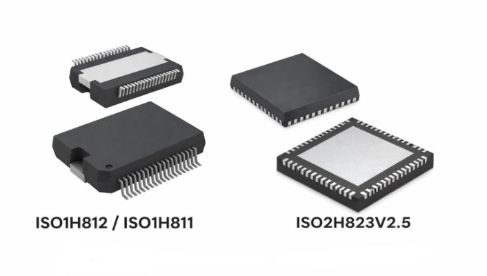
Infineon’s ISO1H812GAUMA1, ISO1H811GAUMA1, and ISO2H823V25XUMA1 are all 8-channel high-side drivers with integrated electrical isolation. Their differentiation is primarily reflected in interface strategy, system-level architectural trade-offs, and the underlying supply/logic platform. This article uses ISO1H812GAUMA1 as the reference and provides a structured comparison to support early-stage design decisions and substitution evaluations.
Parameter Comparison
ISO1H812GAUMA1 | ISO1H811GAUMA1 | ISO2H823V25XUMA1 | |
Number of channels | 8 | 8 | 8 |
Output configuration | High-side | High-side | High-side |
Interface | SPI | Parallel | SPI + Parallel |
Logic supply (Vcc/Vdd) | 3–5.5 V | 3–5.5 V | 2.75–3.6 V |
Isolation capability (typ.) | 500 VAC | 500 VAC | 2500 Vrms |
RDS(on), typ. | 150 mΩ | 150 mΩ | 210 mΩ |
Package | PG-DSO-36 | PG-DSO-36 | PG-VQFN-70-2 |
Application Analysis
- ISO1H812GAUMA1
Best for: Distributed I/O, 24 V output modules, designs with limited isolated-side connector pins, and controller platforms that must scale cleanly across multiple devices.
Insight: A serial interface reduces cross-isolation signal count and associated connector/routing overhead. It also supports a unified software model (e.g., periodic refresh plus state management), enabling more controlled complexity growth when expanding from 8 channels to 16/24/32 channels.
- ISO1H811GAUMA1
Best for: Designs with ample MCU GPIO availability, a preference for intuitive control mapping, and stronger sensitivity to deterministic output update behavior.
Insight: A parallel interface behaves similarly to isolated GPIO, which typically reduces firmware complexity. However, as cross-isolation signal count increases, connector pin planning, PCB routing, and EMC complexity rise materially—particularly when scaling to multi-device architectures.
- ISO2H823V25XUMA1
Best for: Systems standardized on a 3.3 V logic domain, space-constrained PCB designs, and organizations with mature QFN manufacturing and rework capability—especially where diagnostic visibility and maintenance efficiency are prioritized.
Insight: ISO2H823V2.5 can be evaluated as a platform-level option: the logic-voltage domain, package technology, and diagnostic strategy differ from ISO1H81x devices. For architectures moving toward higher integration and faster fault localization, it is often a strong candidate for new designs.
Design Considerations
- Firmware scale and long-term extensibility
SPI-based approach (ISO1H812): Define refresh cadence, communication fault behavior (retain state vs. shutdown vs. safe state), and power-up default output states at the architecture stage to ensure predictable scaling.
Parallel approach (ISO1H811): Firmware logic is typically straightforward; however, long-term expansion is more likely to be constrained by pin/isolated-signal resources and connector space.
- Signal density and system complexity
As the number of cross-isolation signals increases, complexity tends to concentrate in three areas: connector pin allocation, routing return paths, and crosstalk/glitch immunity.
Parallel implementations: Reserve footprints for series resistors, plan signal/ground arrangement carefully, and consider latch/enable mechanisms when necessary to mitigate false triggering due to glitches.
SPI implementations: Focus on clock edge integrity, CS glitch robustness, and readback consistency; additionally, avoid uncontrolled worst-case latency introduced by refresh timing and task scheduling.
- Package and manufacturing implications
PG-DSO-36 (ISO1H811/ISO1H812): Generally favorable for assembly and rework, and well-suited to projects with higher sensitivity to manufacturability and serviceability.
PG-VQFN-70-2 (ISO2H823): Enables a more compact layout; however, thermal pad design, reflow process window, and rework capability should be validated during the design phase.
Replacement & Substitution Recommendations
- ISO1H812GAUMA1 ↔ ISO1H811GAUMA1
Core Difference: Interface type (SPI vs. parallel).
Advice: In most cases, substitution risk is driven less by device-level parameters and more by system resources. Confirm isolated-side signal availability and connector pin budget before adjusting pinout and control logic.
- ISO1H81x (ISO1H811/ISO1H812) ↔ ISO2H823V25XUMA1
Core Difference: Supply domain (5 V-class vs. 3.3 V), package (DSO vs. QFN), and RDS(on).
Advice: Treat this as a cross-platform migration; a PCB redesign is typically unavoidable. Key checks include 3.3 V level compatibility, thermal margin implications (210 mΩ vs. 150 mΩ), and QFN process requirements.
Key Takeaways
- ISO1H812: General-purpose first choice
- ISO1H811: Preferable when system resources are abundant and deterministic updates are the priority
- ISO2H823: Preferable when a 3.3 V + QFN platform direction is prioritized
WIN SOURCE provides stable supply and technical support for Infineon’s ISOFACE™ high-side driver family, including ISO1H812GAUMA1, ISO1H811GAUMA1, and ISO2H823V25XUMA1, supporting both active production and long-lifecycle program requirements.Visit WIN SOURCE for real-time stock and pricing.
©2026 Win Source Electronics. All rights reserved. This content is protected by copyright and may not be reproduced, distributed, transmitted, cached or otherwise used, except with the prior written permission of Win Source Electronics.

COMMENTS