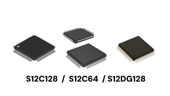
In automotive electronics, industrial control, and embedded systems, 16-bit MCUs remain widely adopted due to their real-time performance, reliability, and mature ecosystems. NXP’s HCS12 architecture, known for its stable instruction set, rich peripherals, and long-term availability, serves as a foundational platform for numerous engineering projects.
While the MC9S12C128CPBE, MC9S12C64CPBE, and MC9S12DG128CFUE all belong to the HCS12 family and share the same core frequency, significant differences exist in memory resources, pin count, and system expandability. In actual projects, relying solely on “same series, same frequency” for substitution often reveals limitations in software space or hardware expansion during later stages.
This article uses the MC9S12C128CPBE as a baseline to compare it with the other two models, providing a reference for engineering design and component substitution evaluation.
Parameter Comparison
MC9S12C128CPBE | MC9S12C64CPBE | MC9S12DG128CFUE | |
Core Speed | 25 MHz | 25 MHz | 25 MHz |
Flash Memory | 128 KB | 64 KB | 128 KB |
RAM | 4KB | 4KB | 8KB |
EEPROM | — | — | 2KB |
I/O Count | 35 | 35 | 59 |
ADC | 8 × 10-bit | 8 × 10-bit | 16 × 10-bit |
Voltage | 3.3V / 5V | 3.3V / 5V | 3.3V / 5V |
Package | 52-LQFP (10×10) | 52-LQFP (10×10) | 80-QFP (14×14) |
Application Analysis
- MC9S12C128CPBE
Best For: Industrial inverters, UPS controllers, CAN bus nodes, and instrumentation.
Insight: This model achieves a balanced configuration regarding Flash capacity, I/O count, and package size. In most practical projects, the 128KB Flash can comfortably accommodate communication protocol stacks (such as CAN, Modbus) and Bootloaders. Engineering experience suggests it provides sufficient margin for future functional expansion, making it a common choice as the starting model for new projects.
- MC9S12C64CPBE
Best For: Relay logic control, simple I/O modules, and high-volume products with fixed features.
Insight: This model is pin-to-pin compatible with the C128. Provided that functional requirements are defined and code size is controlled, it serves as a viable option for reducing BOM costs.
Note: It is generally recommended for use only when the compiled code size is stably below 60KB, leaving a necessary safety margin.
- MC9S12DG128CFUE
Best For: Body Control Modules (BCM), HVAC systems, and multi-sensor data acquisition.
Insight: This model leans more towards system-level integration. Its higher I/O count, double the ADC channels, and independent EEPROM give it a clear advantage in multi-sensor acquisition and scenarios requiring power-down parameter storage. Note that it uses an 80-pin package, making it physically incompatible with the 52-pin C-series for direct replacement.
Design Considerations
- Software Scale & Evolution Space
In engineering planning, Flash capacity selection should be evaluated based on expected functional evolution. If the system has requirements for future feature additions or long-term maintenance, the C128 offers more redundancy compared to the C64. Conversely, the C64 is better suited for applications with clear boundaries that remain unchanged over the long term.
- Analog Signal Density vs. System Complexity
When ADC requirements exceed 8 channels, the DG128 (with 16 ADC channels) allows for a cleaner system architecture than a “C128 + external analog multiplexer” solution. This approach helps reduce the external component count and PCB routing complexity, while also improving analog signal integrity..
- Package Size & PCB Cost
52-LQFP (C Series): Lower pin density makes it suitable for 2-layer PCB designs, with relatively controllable soldering and rework difficulty.
80-QFP (DG Series): Higher pin count may require a higher PCB layer count in some designs to meet routing and signal integrity requirements.
Replacement & Substitution Recommendations
- MC9S12C128CPBE ↔MC9S12C64CPBE
Core Difference: Flash Capacity.
Advice: No hardware modification is required. The focus should be on analyzing the compiled Map file to confirm the program fits within the target Flash space.
- MC9S12C128CPBE ↔MC9S12DG128CFUE
Core Difference: Package, ADC, and EEPROM.
Advice: PCB redesign is required. This path is suitable for scenarios where system functions evolve from a single control node to a complex main controller.
Key Takeaways
- C128: The preferred general-purpose choice
- C64: Cost priority; requires controlled code size
- DG128: Prioritizes interface and analog resources
WIN SOURCE provides stable supply and technical support for the NXP MC9S12 series, covering both active models and long-term project requirements. Whether you need to secure stock for a new design or maintain an existing product line, we help minimize your supply chain risks. Visit WIN SOURCE for real-time inventory and pricing.
©2025 Win Source Electronics. All rights reserved. This content is protected by copyright and may not be reproduced, distributed, transmitted, cached or otherwise used, except with the prior written permission of Win Source Electronics.

COMMENTS