
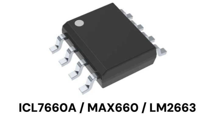
The ICL7660ACBAZA-T, MAX660CSA+T, and LM2663MX/NOPB are all inductorless switched-capacitor voltage converters. With two main external capacitors, each device can be configured to generate a negative supply rail or operate as a positive voltage doubler. Their packages and core pin arrangements are similar, but they should not be treated as simple 45 mA, 100 mA, and 200 mA steps in the same product family. They differ materially in maximum input voltage, internal switch losses, oscillator frequency, external capacitor requirements, control pins, and operating limits.
The engineering question is not simply which device has the highest current rating. The more useful test is whether the negative rail retains enough voltage margin at minimum input voltage, maximum load, worst-case temperature, and the actual ESR of the selected capacitors. Switching frequency, standby power, startup behavior, and PCB layout must also fit the system-level requirements.
Parameter Comparison
| Parameter | ICL7660ACBAZA-T | MAX660CSA+T | LM2663MX/NOPB |
| Input voltage range | 1.5 to 12 V | 1.5 to 5.5 V | 1.5 to 5.5 V (inverter mode) |
| Output-current rating / basis | 20 mA at datasheet test conditions; 45 mA manufacturer parametric rating | 100 mA | 200 mA |
| Typical output resistance | 60 Ω | 6.5 Ω | 3.5 Ω |
| Quiescent current | 80 µA | 120 µA in low-frequency mode; 1 mA in high-frequency mode | 1.3 mA |
| Oscillator / pump frequency | 10 kHz / approx. 5 kHz | 10 or 80 kHz / approx. 5 or 40 kHz | 150 kHz / approx. 75 kHz |
| Shutdown | No | No | Yes; 10 µA shutdown current |
| Operating temperature | 0 to 70 °C | 0 to 70 °C | -40 to 85 °C |
Application Fit
- ICL7660ACBAZA-T
The ICL7660A’s distinguishing advantage is its ability to operate from inputs as high as 12 V. It is well suited to generating a light-load negative bias rail from a 9 V, 10 V, or 12 V bus for instrumentation amplifiers, analog switches, low-speed data-acquisition interfaces, and legacy RS-232 auxiliary supplies. Its 80 µA typical quiescent current also makes it attractive for always-on systems with modest load requirements.
- Best fit: Negative-bias loads from a few milliamps to the low tens of milliamps in 9 V to 12 V systems, where board space is not extremely constrained and capacitors in the 10 µF range are acceptable.
- Poor fit: A 5 V input design that must still deliver approximately -4.5 V at a load near 20 mA. The device’s 60 Ω typical output resistance can consume the available voltage margin quickly.
- Important limits: When VIN is above 3.5 V, the LV pin must be left open. For VIN above 5 V with a fast input rise time, evaluate whether to add the datasheet-recommended external Schottky diode from VOUT to CAP-.
- MAX660CSA+T
The MAX660 uses a higher selectable frequency and larger recommended capacitors to reduce output resistance to the single-digit-ohm range. It is better suited to continuous loads of roughly 20 mA to 100 mA in 3.3 V and 5 V systems, including interface supplies, negative op-amp rails, and internal negative rails in portable instruments.
- Low-frequency mode (approximately 5 kHz pump frequency): Typical quiescent current is 120 µA, which is attractive in battery-powered systems, although larger low-ESR capacitors are generally required.
- High-frequency mode (approximately 40 kHz pump frequency): C1 and C2 can be reduced and the fundamental switching frequency moves above the audio band. The trade-off is an increase in quiescent current to about 1 mA, together with greater sensitivity to layout and high-frequency switching spikes.
- Rating context: The 100 mA capability assumes specific capacitor values and allowable voltage drop. Reusing the ICL7660A’s 10 µF capacitors without selecting high-frequency mode will not reproduce the datasheet’s 6.5 Ω performance.
- LM2663MX/NOPB
The LM2663 targets 200 mA-class loads and system-level power gating. Its 150 kHz oscillator produces an approximately 75 kHz pump frequency, and the device can achieve 3.5 Ω typical output resistance with 47 µF external capacitors. The SD pin also allows the negative rail to be disabled, reducing current to a typical 10 µA when the rail is not required.
- Best fit: Pulsed or continuous loads in the 100 mA to 200 mA range, industrial-temperature environments, and systems that need an MCU to switch the negative rail on and off.
- System-level advantage: Although it has the highest active quiescent current of the three devices, its shutdown function can result in lower average power consumption than a low-frequency device without a shutdown pin when the negative rail has a low duty cycle.
- Trade-off: The approximately 75 kHz pump frequency and higher switch current make input bypassing, the flying-capacitor loop, and ground-return routing more critical. The SD pin must be held reliably low for normal operation.
Design Considerations
- Do not select by maximum output current alone
All three devices are unregulated charge pumps. As load current rises, the output moves toward ground because voltage is lost across the converter’s effective output resistance. Selection should therefore be based on the negative voltage available at the actual load, not on a direct comparison of 45 mA, 100 mA, and 200 mA ratings.
At 5 V input and 20 mA load, a first-order estimate shows substantially more voltage drop with the ICL7660ACBAZA-T than with the MAX660CSA+T or LM2663MX/NOPB. This makes the ICL7660A better suited to light-load auxiliary bias generation than to a higher-current negative rail.
- Frequency drives the power, capacitor, and noise trade-offs
The approximate pump frequencies are 5 kHz for the ICL7660ACBAZA-T, 5 kHz or 40 kHz for the MAX660CSA+T, and 75 kHz for the LM2663MX/NOPB.
A higher switching frequency can reduce output resistance and external capacitor size, but it also increases quiescent current, high-frequency switching spikes, and EMI risk. A lower frequency generally reduces quiescent current, but may require larger capacitors and can place switching noise in the audio band.
- External capacitors directly affect usable output capability
Flying-capacitor and output-capacitor value, ESR, and DC-bias derating all influence voltage drop, ripple, and transient response. The datasheet output-resistance values for these three devices were not measured under identical capacitor and load conditions, so 60 Ω, 6.5 Ω, and 3.5 Ω should not be used by themselves to predict substitution performance.
The final capacitor network should be revalidated at the actual input voltage, load profile, and operating frequency.
- The same package does not mean a drop-in replacement
All three devices are available in 8-pin SOIC packages, but Pin 1 serves a different function on each part:
- ICL7660ACBAZA-T: NC
- MAX660CSA+T: Frequency select
- LM2663MX/NOPB: Shutdown control
The ICL7660ACBAZA-T also supports inputs up to 12 V, whereas the other two devices are limited to 5.5 V. Before approving a replacement, recheck the input-voltage range and the connections to Pin 1, LV, and OSC. Similar package dimensions and core pin placement are not sufficient to establish compatibility.
Selection Recommendations
- VIN may exceed 5.5 V, the load is light, and the negative rail remains on continuously: Choose the ICL7660ACBAZA-T. Budget voltage margin using the 120 Ω worst-case output resistance and account for the LV-pin and fast-power-up requirements.
- VIN is 3.3 V or 5 V, the load is mainly 20 mA to 100 mA, lower voltage drop is required, and the design needs the flexibility to trade off quiescent current, noise, and capacitor size: Choose the MAX660CSA+T.
- VIN is 1.5 V to 5.5 V, the load may reach 100 mA to 200 mA, and the design needs -40 °C to 85 °C operation or MCU-controlled shutdown: Choose the LM2663MX/NOPB. For operation from 1.5 V to 2.5 V, verify performance on actual hardware and against TI’s recommended operating conditions.
- The negative output must remain close to -VIN across the full load range, or the design has tight tolerance or fail-safe requirements: None of these three devices is the ideal choice. Use a closed-loop regulated solution instead.
Product Summary
| Part Number | Manufacturer | Core Positioning | Buy |
| ICL7660ACBAZA-T | Renesas | Light-load negative-voltage converter for designs that prioritize 12 V input capability and low quiescent current | Buy Now |
| MAX660CSA+T | Analog Devices | 100 mA-class solution for 5 V systems, with low output resistance and selectable frequency | Buy Now |
| LM2663MX/NOPB | Texas Instruments | 200 mA-class solution with a wider operating temperature range and low-current shutdown for heavier loads | Buy Now |
WIN SOURCE offers charge pumps and power-management devices from multiple manufacturers for negative-rail generation, interface power, and analog power designs. Visit WIN SOURCE to check real-time inventory for the ICL7660ACBAZA-T, MAX660CSA+T, and LM2663MX/NOPB, and verify their current production status, lifecycle information, and design compatibility before ordering or approving a substitution.
©2026 Win Source Electronics. All rights reserved. This content is protected by copyright and may not be reproduced, distributed, transmitted, cached or otherwise used, except with the prior written permission of Win Source Electronics.

COMMENTS