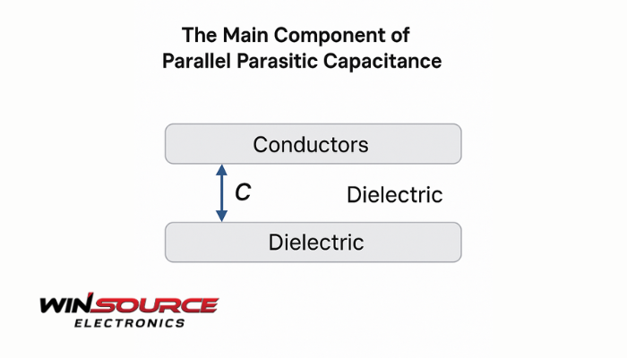
* Question
What is the main component of parallel parasitic capacitance?
* Answer
The main component of parallel parasitic capacitance is the capacitance formed between conductive elements that are at different potentials and are physically adjacent or overlapping, typically in a parallel layout. This unintended capacitance arises due to the electric field coupling between these conductors, and it often affects circuit performance in high-speed or high-frequency applications.
>Key Contributors to Parallel Parasitic Capacitance
h3>>1. Conductor-to-Conductor Overlapp>When two metal traces or electrodes are placed in parallel and separated by a dielectric (e.g., PCB substrate or air), a capacitance forms between them.The larger the overlapping area and the smaller the spacing, the higher the parasitic capacitance.
<>2. Interlayer Capacitance (in multilayer PCBs or ICs)
>Capacitance between traces or planes on adjacent layers (e.g., signal trace over a ground plane) is a major source of parasitic capacitance.Common between power/ground planes and signal layers.
3. Device Junction Capacitance
In semiconductor devices (e.g., MOSFETs), parallel parasitic capacitance can exist between:Gate and source/drain (Cgs, Cgd)
Drain and substrate or adjacent structures.
These capacitances affect switching speed and are modeled in device-level simulations.
4. Capacitive Coupling Between PCB Traces
Closely spaced parallel traces on a PCB or flexible substrate result in trace-to-trace coupling.This is a form of parasitic capacitance and a primary concern in high-speed digital or RF layout.
Simplified Equation
For two parallel conductors:C=ε⋅A/d
Where:
C = Capacitance (F)
ε = Permittivity of the dielectric material
A = Overlapping area
d = Distance between conductors