* Question
What is the main component of parallel parasitic capacitance?
* Answer
The main component of parallel parasitic capacitance is the capacitance formed between conductive elements that are at different potentials and are physically adjacent or overlapping, typically in a parallel layout. This unintended capacitance arises due to the electric field coupling between these conductors, and it often affects circuit performance in high-speed or high-frequency applications.
Table of Contents
ToggleKey Contributors to Parallel Parasitic Capacitance
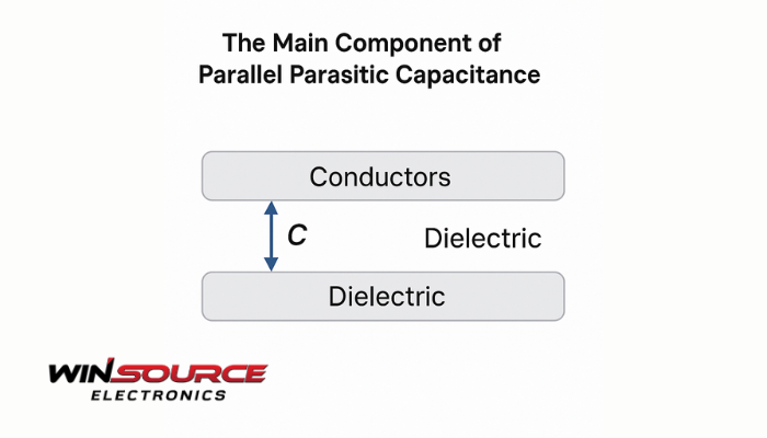
1. Conductor-to-Conductor Overlap
When two metal traces or electrodes are placed in parallel and separated by a dielectric (e.g., PCB substrate or air), a capacitance forms between them.
The larger the overlapping area and the smaller the spacing, the higher the parasitic capacitance.
2. Interlayer Capacitance (in multilayer PCBs or ICs)
Capacitance between traces or planes on adjacent layers (e.g., signal trace over a ground plane) is a major source of parasitic capacitance.
Common between power/ground planes and signal layers.
3. Device Junction Capacitance
In semiconductor devices (e.g., MOSFETs), parallel parasitic capacitance can exist between:
Gate and source/drain (Cgs, Cgd)
Drain and substrate or adjacent structures.
These capacitances affect switching speed and are modeled in device-level simulations.
4. Capacitive Coupling Between PCB Traces
Closely spaced parallel traces on a PCB or flexible substrate result in trace-to-trace coupling.
This is a form of parasitic capacitance and a primary concern in high-speed digital or RF layout.
Simplified Equation
For two parallel conductors:
C=ε⋅A/d
Where:
C = Capacitance (F)
ε = Permittivity of the dielectric material
A = Overlapping area
d = Distance between conductors
Conclusion
The main component of parallel parasitic capacitance arises from the capacitive coupling between adjacent or overlapping conductors—whether they are PCB traces, IC interconnects, or device terminals. Managing this capacitance is critical in high-speed and precision analog circuits to avoid signal distortion, crosstalk, and timing errors. Careful layout design, spacing, and use of ground shielding are common techniques to minimize its impact.
COMMENTS