Overview
TPD2E001DRLR is a dual-channel, low-capacitance TVS (transient voltage suppression) diode array launched by Texas Instruments, designed for ESD (electrostatic discharge) protection of high-speed data lines and sensitive signal interfaces. The device complies with the IEC 61000-4-2 ESD standard, provides ±15kV (air discharge) and ±8kV (contact discharge) protection, and has extremely low parasitic capacitance (only 0.5pF), making it very suitable for USB, HDMI, DisplayPort, antenna, button interface and other high-speed I/O pin protection.
Specifications
parameter | Numeric |
Number of channels | 2-way |
Reverse breakdown voltage (typical) | 6.1V |
Clamping voltage (typical @8kV) | 11V |
Leakage current (max) | 1nA @ 5.5V |
Input capacitance (typical) | 0.5pF |
ESD protection level | ±15kV (air) / ±8kV (contact) |
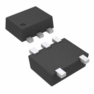
Package Type | SOT-5 (DRL package) |
Operating voltage range | 0V to 5.5V |
Operating temperature range | –40°C to +85°C (Industrial) |
Comply with standards | IEC 61000-4-2, IEC 61000-4-4 |
Key features of TPD2E001DRLR
Dual-channel ESD protection, suitable for high-speed data lines
Suitable for protecting two signal lines such as USB D+/D-, HDMI channel, key input, capacitive touch interface, etc., saving board space.
Ultra-low input capacitance (0.5pF)
The extremely low parasitic capacitance ensures that signal integrity is not disturbed, making it ideal for protecting high-speed communication interfaces ranging from hundreds of MHz to GHz.
Strong ESD suppression capability
It provides ±15kV (air) / ±8kV (contact) protection in accordance with IEC61000-4-2 standard and is suitable for interface areas with frequent human-machine contact, such as USB sockets, buttons, antenna terminals, etc.
Fast response and low clamping voltage
The transient response speed is fast, and it can quickly clamp the electrostatic spike voltage to a safe level, thus protecting the subsequent circuits to the maximum extent.
Small package, suitable for high-density layout
Using SOT-5 (DRLR) package, it occupies a small PCB area and is suitable for ultra-thin devices, portable products and compact designs.
Wide operating voltage range and very low leakage current
It operates stably in a 0–5.5V power supply system, with a typical leakage current of 1nA. It can be directly connected in parallel to the I/O interface with almost no impact on normal operation.
Typical application scenarios
The high performance ESD suppression and low capacitance of the TPD2E001DRLR make it ideal for the following applications:
USB port protection (USB 2.0 / USB OTG)
Protect the USB D+/D- data line to prevent chip damage caused by plugging or unplugging or human static electricity.
HDMI / DisplayPort video interface
Avoid high frequency signal distortion and protect against ESD shock at the interface.
Button and touch screen interface protection
Provides front-end electrostatic protection to improve the reliability of the device in human-computer interaction scenarios.
Antenna port/RF interface protection
Provides electrostatic surge protection without affecting RF signal transmission.
General high-speed GPIO, control line protection
Used for GPIO or control interface of MCU and FPGA to improve the overall system EMC performance.
Advantages comparison analysis
Features/Specifications | TPD2E001DRLR | Common TVS tube |
Number of channels | 2-way | 1 or more |
Input Capacitance | 0.5pF | 3pF – 20pF |
Clamping voltage (typical) | 11V | 20V or more |
Response speed | Nanosecond level | Microseconds (some slower) |
Package size | Small SOT-5 | SMA/SMB (larger) |
Is it designed for high-speed signals? | yes | no |
The TPD2E001DRLR has significant advantages in capacitance, speed and clamping performance, making it an ideal ESD protection solution for modern high-speed signal interfaces.
Manufacturer introduction: Texas Instruments (TI)
TI is a leading global analog and embedded semiconductor manufacturer, providing complete system-level protection device solutions. As its professional ESD suppression product line, the TPD2E001 series is widely used in consumer electronics, industry, automobiles and other fields, helping customers improve system anti-interference performance without sacrificing signal integrity.
Why choose TPD2E001DRLR?
● Supports ±15kV air discharge/±8kV contact discharge (compliant with IEC standards)
● Ultra-low capacitance (0.5pF), will not affect high-speed interface performance
● Provides dual-channel protection, saves space and reduces costs
● Low clamping voltage + fast response, effectively protects subsequent chips
● Small package (SOT-5), suitable for high-density circuit design
● Working voltage up to 5.5V, supports mainstream interfaces such as USB, HDMI, GPIO, etc.
FAQ
Q1: Can TPD2E001DRLR be used for USB3.0 interface?
A: It is not recommended . The typical input capacitance of TPD2E001DRLR is about 1.5pF. Although it is suitable for ESD protection of high-speed interfaces such as USB 2.0, its capacitance value may affect the signal integrity for signal lines of USB 3.0 and above. The operating frequency of USB 3.0 interface is as high as 5Gbps, and the parasitic capacitance requirements of ESD protection devices are more stringent (generally recommended to be <0.3pF). Therefore, TI officially recommends using devices with lower capacitance designed for USB 3.x, such as TPD4E02B04 or TPD1E10B06 series, to ensure that the quality of high-speed signal transmission is not disturbed.
Q2: Is the pin connection of TPD2E001DRLR directional?
A: It is directional . TPD2E001DRLR is designed based on a unidirectional TVS (transient voltage suppression) structure. Each channel consists of two pins: one connects the protected signal line and the other connects to ground (GND). To achieve effective surge voltage clamping protection, it must be correctly connected according to the pin configuration provided in the TI data sheet to ensure that the signal enters from the “IO” end and is clamped at the “GND” end. If the direction is connected incorrectly, the normal ESD suppression effect will not be achieved, and it may even affect the reliability of the device itself.
For more details and to explore our inventory, please visit the links below:
Product Details: Win Source – TPD2E001DRLR
Quote: Win Source – TPD2E001DRLR
©2025 Win Source Electronics. All rights reserved. This content is protected by copyright and may not be reproduced, distributed, transmitted, cached or otherwise used, except with the prior written permission of Win Source Electronics.
COMMENTS