* Question
What Are the Features of SignalTap II Logic Analyzer?
* Answer
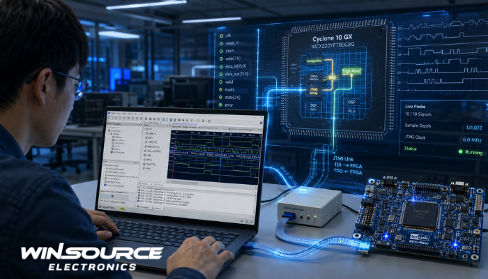
SignalTap II Logic Analyzer is an embedded debugging tool provided in Intel (Altera) Quartus Prime software. It allows engineers to observe real-time internal signals inside an FPGA without using external test equipment or additional I/O pins.
It works like an on-chip logic analyzer, making FPGA debugging much faster and more efficient.
Key Features of SignalTap II
1. Real-Time Internal Signal Observation
SignalTap II can capture and display internal FPGA signals during actual hardware operation.
- No need to route signals to external pins
- Debug “inside the chip” while running at full speed
- Helps verify post-synthesis behavior
2. Embedded Logic Analyzer Architecture
SignalTap II is implemented directly inside the FPGA.
- Uses FPGA logic resources (LUTs, registers, RAM blocks)
- Captured data is stored in on-chip memory
- Data is transferred to PC via JTAG interface
This makes it a true hardware-based debugging tool, not a simulation.
3. Trigger-Based Data Capture
It supports flexible trigger conditions to start data acquisition:
- Simple logic triggers (AND / OR conditions)
- Edge detection (rising/falling edge)
- Multi-level advanced triggering (sequential events)
This helps capture only meaningful signal activity instead of continuous noise.
4. Deep Sample Buffer (Configurable Capture Depth)
Users can define how many samples to store:
- Small depth → lower FPGA resource usage
- Large depth → longer time window of captured data
Typical use cases balance between visibility and resource consumption.
5. Multiple Signal and Bus Monitoring
SignalTap II supports:
- Single-bit signals
- Multi-bit buses (data paths, addresses, control signals)
- Custom grouping and formatting (signed/unsigned, hex, ASCII, etc.)
This makes it suitable for both control logic and data-heavy debugging.
6. Flexible Trigger Modes
It provides multiple trigger modes:
- Basic trigger (single condition)
- Sequential trigger (multi-step event detection)
- State-based trigger (complex system behavior analysis)
This is especially useful for debugging FSMs and protocol logic.
7. On-Chip Resource Utilization
Because it is embedded, it uses FPGA resources:
- Logic elements (LEs)
- Block RAM (M9K/M10K, etc.)
- Routing resources
Important trade-off:
More debugging signals = more resource usage and longer compilation time.
8. No Need for External Debug Hardware
SignalTap II eliminates the need for:
- External logic analyzers
- Extra I/O pin routing
- PCB signal probing for internal nodes
All data is accessed via a standard JTAG download cable.
9. Data Export and Offline Analysis
Captured waveform data can be exported:
- CSV (for MATLAB / Python analysis)
- VCD (for simulation tools)
- Image formats for documentation
This helps in post-processing and system-level debugging.
10. Multiple Instance Support
You can instantiate multiple SignalTap analyzers in one design:
- Monitor different subsystems simultaneously
- Apply different trigger conditions per instance
- Debug complex SoC-level FPGA designs
Summary
SignalTap II is a powerful FPGA debugging tool with these core features:
- Real-time internal signal visibility
- Embedded on-chip logic analyzer structure
- Flexible trigger mechanisms
- Configurable deep data capture
- Multi-signal/bus monitoring
- JTAG-based data extraction
- No external hardware required
Conclusion
SignalTap II is essentially a built-in FPGA oscilloscope for digital logic, enabling engineers to debug hardware behavior directly inside the chip. It bridges the gap between simulation and real-world operation, making it a critical tool for FPGA development and verification.