* Question
What are the main steps of the lithography process?
* Answer
The lithography process is a fundamental technique in semiconductor fabrication used to transfer patterns onto a wafer surface. These patterns define the intricate structures of integrated circuits (ICs), such as transistors, interconnects, and vias. The process is highly precise and is repeated multiple times throughout chip manufacturing.
Here is a structured overview of the main steps in the lithography process:
Table of Contents
Toggle1. Wafer Preparation
Cleaning: The silicon wafer is thoroughly cleaned to remove particles, organic residues, or metal contamination.
Dehydration Bake: Removes moisture from the wafer surface to enhance photoresist adhesion.
Adhesion Promotion: Application of an adhesion promoter (e.g., HMDS) to improve photoresist uniformity.
2. Photoresist Coating
Spin Coating: A thin, uniform layer of photoresist (a light-sensitive polymer) is applied by spinning the wafer at high speed.
Thickness Control: The spin speed and resist viscosity determine the film thickness, typically in the range of 0.1 to 2 µm.
3. Soft Bake (Prebake)
Purpose: Evaporates solvent from the photoresist and enhances adhesion.
Temperature: Typically 90–110°C on a hot plate or in a convection oven.
Effect: Reduces resist flow during exposure and improves resolution.
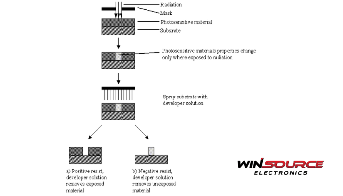
4. Mask Alignment and Exposure
Mask (Photomask or Reticle): Contains the desired circuit pattern in the form of opaque and transparent regions.
Alignment: The mask is aligned with the wafer so that patterns from previous layers match precisely.
Exposure: UV light (commonly 248 nm or 193 nm) is projected through the mask onto the photoresist.
Positive resist becomes soluble where exposed to light.
Negative resist becomes insoluble where exposed.
5. Post-Exposure Bake (PEB)
Purpose: Stabilizes the photo-induced chemical changes in the resist and reduces standing wave effects.
Typical Use: Especially important in chemical amplification resists used for deep UV (DUV) lithography.
6. Development
Developer Solution: Typically an aqueous alkaline solution (e.g., TMAH) is used to dissolve the exposed (or unexposed, depending on resist type) photoresist.
Development Time: Carefully controlled to preserve pattern fidelity.
Rinse and Dry: The wafer is rinsed with deionized water and dried after development.
7. Pattern Inspection and Critical Dimension (CD) Measurement
Metrology: The patterned resist is inspected under an optical or SEM tool to verify linewidths and alignment accuracy.
CD Control: Ensures that dimensions match the design rules within tolerance limits.
8. Etching or Implantation
The developed pattern acts as a mask for subsequent processes like:
Etching: Transfers the pattern into the underlying material (oxide, metal, or silicon) using plasma or wet etching.
Ion Implantation: Introduces dopants into exposed areas for junction formation.
9. Photoresist Removal (Strip)
Process: After etching or implantation, the remaining photoresist is removed using:
Plasma ashing (O₂ plasma)
Wet stripping with solvents or chemical strippers
Clean Surface: The wafer is cleaned again to prepare for the next lithography cycle.
10. Repeat Process
Lithography is a multi-layer process. The above steps are repeated for each layer of the IC, sometimes 30–50 times, depending on design complexity.
Insight
The lithography process is a critical determinant of chip resolution, yield, and performance. It combines chemistry, optics, and mechanical precision. Modern techniques such as immersion lithography, extreme ultraviolet (EUV), and multiple patterning are continuously evolving to enable sub-10 nm nodes.
COMMENTS