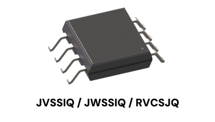
The W25Q64JVSSIQ, W25Q64JWSSIQ, and W25Q64RVCSJQ are 64-Mbit Serial NOR flash devices from Winbond. They can store boot code, system firmware, configuration parameters, and other non-volatile data. Their main selection differences are supply voltage, read performance, power consumption, operating temperature, and interface support.
Parameter Comparison
| Parameter | W25Q64JVSSIQ | W25Q64JWSSIQ | W25Q64RVCSJQ |
| Memory organization | 64 Mbit; 256 B/page | 64 Mbit; 256 B/page | 64 Mbit; 256 B/page |
| Supply voltage | 2.7–3.6 V | 1.7–1.95 V | 2.7–3.6 V |
| Interface modes | SPI, Dual SPI, Quad SPI | SPI, Dual SPI, Quad SPI | SPI, Dual SPI, Quad SPI, QPI |
| Maximum read frequency | 133 MHz | 133 MHz | 166 MHz |
| Erase sizes | 4/32/64 KB | 4/32/64 KB | 4/32/64 KB |
| Page program time | 0.4 ms typ. | 0.8 ms typ. | 0.18 ms typ. |
| Deep power-down current | 1 µA typ. | 0.1 µA typ. | 0.1 µA typ. |
| Operating temperature | −40°C to +85°C | −40°C to +85°C | −40°C to +105°C |
| Package | SOIC-8, 208 mil | SOIC-8, 208 mil | SOP-8, 208 mil |
Application Fit
- W25Q64JVSSIQ
Best for: General embedded products using a 3.3 V MCU or SoC, including industrial controllers, smart-home equipment, IoT gateways, display modules, and networking devices.
Key takeaway: This device is suited to established platforms developed around the W25Q-JV or W25Q-FV families. The Q-suffix device has QE fixed at 1, so Quad I/O commands can be used without programming the QE bit; the /HOLD function is unavailable.
- W25Q64JWSSIQ
Best for: Wearables, portable terminals, and low-power IoT nodes using a 1.8 V supply and I/O domain.
Key takeaway: This device focuses on low-voltage and low-power operation. It must not be connected directly to a 3.3 V supply or logic interface. Migration from the JV family requires a review of host I/O levels and power-up timing.
- W25Q64RVCSJQ
Best for: New 3 V systems that require higher read performance, faster programming, or operation at temperatures up to 105°C.
Key takeaway: This device supports QPI and Flex Block/Sector Protection. Operation at 166 MHz depends on the command, dummy-cycle configuration, and address alignment. The Q-suffix version does not support DTR; an M-suffix device should be evaluated when DTR is required.
Design Considerations
- Confirm supply and I/O voltage first
The JW family operates at 1.8 V and cannot be substituted for a JV or RV device based only on capacity and package. Separate power domains or level translation may be required when the host and flash use different I/O voltages.
- Do not compare maximum frequency alone
The W25Q64JVSSIQ reaches 133 MHz at 3.0–3.6 V, while the corresponding limit is generally 104 MHz at 2.7–3.0 V. The W25Q64JWSSIQ reaches 133 MHz only with the specified Quad I/O read mode and temperature conditions.
The W25Q64RVCSJQ requires additional dummy cycles and a four-byte-aligned starting address to reach 166 MHz. Reads from an arbitrary address are generally limited to 133 MHz. The final clock setting should reflect the selected command, operating conditions, and PCB signal integrity.
- Check interface and software compatibility
The three devices do not use identical device IDs, status-register settings, protection mechanisms, or read configurations. Migration should include verification of the QE state, JEDEC ID, dummy cycles, reset sequence, program and erase timeouts, and support in the boot ROM or flash driver.
- Similar packages do not establish drop-in compatibility
All three devices use 8-pin, 208-mil packages, but their package codes differ. Mechanical dimensions, land patterns, and pin functions should still be checked. System timeouts should also be based on the maximum program and erase times specified in the datasheet rather than typical values.
Product Summary
| Part | Manufacturer | Recommended use | Buy |
| W25Q64JVSSIQ | Winbond | General 3 V option for established SPI and Quad SPI platforms | Buy Now |
| W25Q64JWSSIQ | Winbond | 1.8 V option for low-power systems | Buy Now |
| W25Q64RVCSJQ | Winbond | Newer 3 V option with wider temperature and higher performance | Request a Quote |
Select the device according to host I/O voltage, interface mode, read conditions, temperature range, and software compatibility. Visit WIN SOURCE to check current inventory and pricing.
©2026 Win Source Electronics. All rights reserved. This content is protected by copyright and may not be reproduced, distributed, transmitted, cached or otherwise used, except with the prior written permission of Win Source Electronics.