
What are the two basic communication methods for serial communication?
The two basic communication methods for serial communication are:
- Synchronous Serial Communication: In synchronous serial communication, data is transmitted in a continuous stream of bits. A clock signal is used to synchronize the sending and receiving devices. Both the sender and receiver must be synchronized with the same clock signal to ensure accurate data transmission. Synchronous serial communication is typically faster and more reliable than asynchronous serial communication.
- Asynchronous Serial Communication: In asynchronous serial communication, data is transmitted as individual characters or bytes with start and stop bits framing each character. Unlike synchronous communication, there is no continuous clock signal to synchronize the devices. Instead, the receiver detects the start and stop bits to determine the boundaries of each character. Asynchronous serial communication is commonly used for lower data rates and simpler communication setups.
Both synchronous and asynchronous serial communication methods have their advantages and are used in different applications based on factors such as data rate, complexity, and reliability requirements.
What is the difference between active and passive drives?
In the context of electronics or mechanical systems, the terms “active drive” and “passive drive” refer to different methods of controlling or powering a device. Here’s an explanation of the difference between the two:
- Active Drive: Active drive refers to a system where an external power source actively supplies energy to drive or control a device. The active drive source actively generates and provides the necessary power or signals required for the device’s operation. It typically involves the use of active components such as transistors, amplifiers, or power sources to deliver the required energy. Active drives are capable of actively manipulating and controlling the behavior of the driven device.
- Passive Drive: Passive drive, on the other hand, relies on external forces or energies without actively providing power or control signals. It utilizes passive components that do not actively amplify or generate power but rather respond to and utilize existing energies or signals. Passive drives often involve the transfer or conversion of energy from one form to another.
Examples of passive drive include a windmill or water wheel being driven by wind or water currents to produce mechanical energy, or a simple resistor-capacitor (RC) circuit that relies on the charging and discharging of the capacitor using existing signals.In summary, active drives actively generate or provide power to drive and control a device, while passive drives utilize existing energies or signals without actively generating power.
Increase the energy density of EDLC devices.There are three main methods, what are they?
To increase the energy density of Electric Double Layer Capacitor (EDLC) devices, there are three main methods commonly employed:
- Electrode Material Optimization: One approach is to optimize the materials used for the electrodes in EDLCs. The energy density of an EDLC is directly influenced by the specific surface area of the electrode materials. Increasing the specific surface area allows for more effective ion adsorption, leading to higher energy storage capacity. Researchers have been exploring various high-surface-area materials such as carbon nanotubes, graphene, activated carbon, and other nanomaterials to enhance the energy density of EDLCs.
- Electrolyte Optimization: The choice of electrolyte also plays a crucial role in improving the energy density of EDLCs. The electrolyte facilitates ion transport between the electrodes, affecting the capacitance and energy storage capabilities. By optimizing the composition and properties of the electrolyte, such as using higher-concentration electrolytes or ionic liquids, researchers aim to enhance the charge storage capacity and overall energy density of the EDLC device.
- Device Architecture and Engineering: Another method involves optimizing the overall device architecture and engineering. This includes improving the design and configuration of the EDLC, such as electrode arrangement, separator materials, and cell configuration. For example, using asymmetric electrode configurations, where one electrode has a larger surface area, can enhance the energy density. Additionally, advancements in manufacturing techniques, such as electrode patterning and 3D structures, have shown promise in increasing the energy density of EDLC devices.
These methods are continuously researched and developed to improve the energy density of EDLCs, making them more competitive with other energy storage technologies.
What are the Virtex class chips?
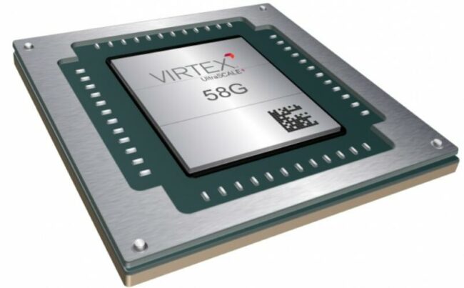
Virtex is a series of field-programmable gate array (FPGA) chips developed by Xilinx, a leading manufacturer of programmable logic devices. The Virtex family of chips is known for its high-performance capabilities and versatility, making them suitable for a wide range of applications.
The Virtex FPGA chips offer a combination of configurable logic blocks, embedded memory, digital signal processing (DSP) capabilities, and high-speed serial transceivers. They are designed to provide flexible and reconfigurable hardware solutions, allowing designers to implement complex digital circuits and systems.The Virtex family has gone through several generations of advancements, with each generation introducing new features and improvements. Some of the notable Virtex chip families include:
- Virtex-7: The Virtex-7 family was one of the most recent generations (prior to my knowledge cutoff in September 2021). It offered high-performance FPGAs with advanced features such as high-speed serial transceivers, improved DSP capabilities, and significant logic capacity.
- Virtex UltraScale and UltraScale+: The UltraScale and UltraScale+ families are subsequent generations of Virtex chips, offering even higher performance, improved power efficiency, and enhanced functionality. These chips incorporate advanced technologies such as 3D stacked silicon interconnects, fine-grained programmable interconnects, and heterogeneous system integration.
- Virtex-6, Virtex-5, and earlier generations: These earlier Virtex families also provided high-performance FPGA solutions and were widely used in various industries and applications.
It’s worth noting that Xilinx, the manufacturer of Virtex chips, was acquired by Advanced Micro Devices (AMD) in 2020. As a result, the future developments and product roadmap for the Virtex family may be subject to changes influenced by AMD’s strategies and priorities.
The reset causes the microcontroller to quickly enter the initial state and execute the program from this state.What are the main effects of reset?
The main effects of a reset on a microcontroller are as follows:
- Program Counter (PC) Reset: The program counter, which keeps track of the memory address of the next instruction to be executed, is typically reset to the initial address. This causes the microcontroller to start executing the program from the beginning, as if it were powering up for the first time.
- Registers Reset: Depending on the microcontroller architecture, certain registers may be cleared or initialized to their default values during a reset. This ensures a known and consistent starting state for the execution of the program.
- Peripherals Reset: In some microcontrollers, a reset can also affect the state of various peripheral modules integrated within the microcontroller. These peripherals may be reset, re-initialized, or put into a default state, depending on the specific microcontroller design.
- Timers and Counters Reset: Resetting a microcontroller often includes resetting any timers or counters that may be in use. This clears their current values and restarts them from the beginning.
- I/O Pins Configuration: Some microcontrollers may reset the configuration of input/output (I/O) pins to a default state. This ensures that the pins are not in any unintended state at the start of the program.
- Power-On Reset (POR) Circuit: Many microcontrollers have a dedicated Power-On Reset (POR) circuit that generates a reset signal when power is initially applied to the device. This POR circuit ensures a controlled and predictable startup state for the microcontroller.
Resetting a microcontroller is commonly used to initiate a clean and predictable system state, allowing the program to start execution from a known starting point. It helps to handle unexpected conditions, recover from errors, or perform system initialization tasks when necessary.
What are the applications of FPGAs in wireless communication systems?
FPGAs (Field-Programmable Gate Arrays) find a range of applications in wireless communication systems due to their flexibility, high processing power, and ability to implement complex digital logic. Here are some common applications of FPGAs in wireless communication:
- Baseband Processing: FPGAs are widely used for baseband processing in wireless communication systems. They can handle tasks such as modulation and demodulation, error correction coding and decoding, channel estimation, equalization, and filtering. The reconfigurable nature of FPGAs allows for efficient implementation of these signal processing algorithms, enabling real-time data processing in wireless systems.
- Wireless Protocols: FPGAs are used to implement various wireless communication protocols, such as Wi-Fi (IEEE 802.11), cellular standards (e.g., 3G, 4G/LTE, 5G), Bluetooth, Zigbee, and more. FPGAs offer the flexibility to adapt and update these protocols as standards evolve, making them suitable for software-defined radio (SDR) applications.
- Digital Front-End (DFE): FPGAs can be employed for implementing the digital front-end of wireless transceivers. This includes functions like digital upconversion, digital downconversion, quadrature modulation/demodulation, synchronization, and carrier frequency recovery. FPGAs allow for the efficient integration of these functions into a single chip, reducing the need for external components.
- Multiple-Input Multiple-Output (MIMO) Systems: MIMO techniques are widely used in wireless communication to enhance data throughput and link reliability. FPGAs can be utilized to implement MIMO signal processing algorithms, such as MIMO channel estimation, beamforming, and spatial multiplexing, enabling efficient utilization of multiple antennas at both transmitter and receiver ends.
- Software-Defined Radio (SDR): FPGAs are well-suited for SDR platforms, where the radio functionality can be implemented and reconfigured in software. FPGAs enable the flexibility to support multiple wireless standards, dynamic spectrum access, and waveform adaptation, making them ideal for software-defined radio applications.
- Test and Measurement: FPGAs are used in wireless test and measurement equipment to generate and analyze signals. They can implement signal generators, digital signal analyzers, and protocol-specific testing functions, enabling efficient characterization, testing, and validation of wireless devices and systems.
These are just a few examples of the applications of FPGAs in wireless communication systems. The versatility and programmability of FPGAs make them a valuable tool for implementing complex digital processing tasks in wireless technologies.
What is the security system of the smart card?
The security system of a smart card is designed to protect the confidentiality, integrity, and authenticity of the data stored on the card and to ensure secure transactions. Here are some key elements of a smart card’s security system:
- Physical Security: Smart cards are tamper-resistant and have physical security features to protect against unauthorized access. This includes the use of materials that are difficult to tamper with, such as hard plastic casing, embedded chips, and secure contact points.
- Authentication and Encryption: Smart cards employ authentication mechanisms to verify the identity of the card and the cardholder. This typically involves the use of cryptographic algorithms and keys stored on the card. Encryption is used to protect sensitive data during transmission and storage, ensuring that only authorized parties can access and understand the information.
- Secure Data Storage: Smart cards have secure memory areas, such as protected memory or secure elements, to store sensitive data, cryptographic keys, and authentication credentials. These memory areas are designed to be resistant to unauthorized access or extraction of data.
- PIN Protection: Smart cards often require a Personal Identification Number (PIN) to be entered by the cardholder as an additional layer of security. The PIN acts as a password and is used to authenticate the cardholder’s identity before allowing access to the card’s functions and data.
- Secure Communication Protocols: Smart cards use secure communication protocols to interact with card readers or terminals. These protocols ensure the integrity and confidentiality of the exchanged data and protect against eavesdropping or tampering.
- Application Firewall: Smart cards can have an application firewall that isolates different applications and prevents unauthorized access between them. This helps to ensure that one application’s data cannot be accessed or modified by another application without proper authorization.
- Secure Key Management: Smart cards employ secure key management techniques to protect cryptographic keys and ensure their secure generation, storage, and usage. This includes mechanisms for key generation, key diversification, key wrapping, and secure key exchange protocols.
These security measures collectively provide robust protection against unauthorized access, data theft, and tampering in smart card systems. It’s important to note that the specific security features and implementations may vary depending on the type of smart card and its intended use (e.g., payment cards, identification cards, access control cards, etc.).
What are the functions of the dead zone (DB) module?
The Dead Zone (DB) module, also known as the Dead Time module, is a component commonly found in motor control systems, particularly in applications involving power electronic devices such as inverters or motor drives. The main function of the Dead Zone module is to introduce a small delay or dead time between the switching of two power devices (such as transistors or MOSFETs) to prevent shoot-through current and improve system reliability. Here are the primary functions of the Dead Zone module:
- Shoot-through Prevention: The Dead Zone module ensures that there is a delay or dead time between turning off one power device and turning on the complementary power device in a bridge configuration. This dead time prevents both power devices from conducting simultaneously, which would result in a short circuit or shoot-through current. Shoot-through can cause excessive power dissipation, damage to the power devices, and inefficient operation of the motor control system.
- Minimization of Transient Overlaps: During the switching transition of power devices, there may be brief periods where both devices are partially conducting, resulting in transient overlaps. These overlaps can lead to spikes in current or voltage, causing undesirable effects such as increased switching losses, electromagnetic interference (EMI), and motor control instability. The Dead Zone module helps minimize such overlaps by introducing a controlled delay between the switch transitions.
- Protection against Voltage Spikes: The Dead Zone module also helps protect against voltage spikes that may occur during switching. By ensuring that both power devices are not simultaneously conducting, it reduces the chances of voltage spikes and the associated stress on the system components.
- Improved System Reliability: By preventing shoot-through currents and reducing transient overlaps, the Dead Zone module contributes to improved system reliability and longevity. It helps maintain the integrity of the power devices, reduces stress on the circuit components, and ensures stable and efficient operation of the motor control system.
The duration of the dead zone or dead time introduced by the module is typically configurable and depends on the specific requirements of the motor control application, the characteristics of the power devices, and the desired system performance.
What are the commonly used low frequency tags?
Low-frequency (LF) tags are a type of RFID (Radio Frequency Identification) tags that operate at lower frequencies, typically between 125 kHz and 134 kHz. These tags are commonly used in various applications that require close-range identification and tracking. Some commonly used low-frequency tags include:
- LF 125 kHz Tags: LF tags operating at 125 kHz are widely used for access control systems, animal identification, and asset tracking. They are often used in proximity cards and key fobs for building access, where the tag is brought close to a reader for authentication.
- LF 134 kHz Tags: LF tags operating at 134 kHz are utilized in applications such as livestock tracking, pet identification, and industrial asset management. These tags are commonly implanted or attached to animals or objects and can be read by compatible LF readers in close proximity.
- LF Glass Tags: LF glass tags, also known as glass transponders or bio-glass tags, are small cylindrical tags typically enclosed in a biocompatible glass capsule. These tags are commonly used in animal identification, particularly for permanent identification in pets, livestock, and laboratory animals.
- LF Disc Tags: LF disc tags are thin, round tags that are commonly used in applications such as logistics, inventory management, and access control. These tags can be attached to objects or embedded into products for identification and tracking purposes.
- LF Wristband Tags: LF wristband tags are wearable tags designed to be worn on the wrist, commonly used in applications like event management, healthcare, and access control. These tags are convenient for identification and tracking of individuals in various environments.
It’s important to note that the specific LF tags used can vary depending on the requirements of the application, the desired read range, the type of objects being tagged, and the compatibility with LF readers and systems.
How does the cookie data move?
Cookie data moves through a process that involves several steps and components. Here’s an overview of how cookie data moves:
- Client Request: When a user’s web browser sends a request to a web server, it includes various headers, including the Cookie header. The Cookie header contains one or more cookies associated with the website or domain being accessed.
- Server Response: Upon receiving the client request, the web server processes the request and generates a response. If the server needs to send a cookie to the client, it includes a Set-Cookie header in the response.
- Cookie Storage: The web browser receives the server response, including the Set-Cookie header if applicable. The browser then stores the cookie data locally on the user’s device. The storage mechanism varies based on the browser, but typically the cookies are stored in a cookie file or in-memory storage.
- Subsequent Requests: When the user interacts with the website and sends subsequent requests, the browser automatically includes the stored cookies in the Cookie header of each request. This allows the server to identify and authenticate the user, personalize the user’s experience, or maintain session information.
- Server Processing: The web server receives subsequent requests from the client, including the Cookie header. It can then access and utilize the cookie data to provide personalized content, remember user preferences, maintain session state, or perform other operations based on the information stored in the cookies.
It’s important to note that cookies are domain-specific and have limitations on their scope. Cookies are typically associated with a specific domain or subdomain, and they are sent to the server only when making requests to that domain or subdomain. Additionally, cookies can have attributes such as expiration date, secure flag (for HTTPS-only communication), and path restrictions, which further define their behavior and usage.Overall, the movement of cookie data involves the exchange of information between the client (web browser) and the server, enabling the server to maintain state and personalize the user’s browsing experience.
COMMENTS