In relay, solenoid, indicator, LED display, and small-motor control circuits, an MCU or logic controller usually cannot drive higher-voltage, higher-current loads directly. A low-side driver is therefore required to provide an interface between low-level logic and higher-power loads.
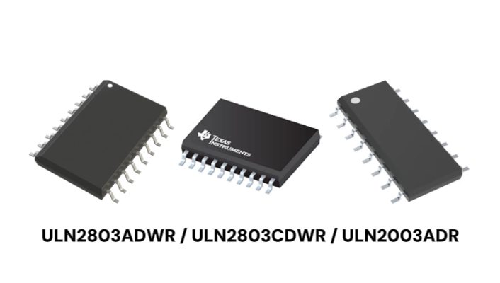
Texas Instruments’ ULN2803ADWR, ULN2803CDWR, and ULN2003ADR are NPN Darlington transistor arrays. Each device provides open-collector low-side outputs and integrated clamp diodes for inductive loads. Their output-voltage ratings, current ratings, and input structures are broadly similar. The main differences are channel count, package and pinout, operating-temperature range, and product lifecycle status.
This guide uses the discontinued ULN2803ADWR, which remains common in legacy equipment, as the baseline. It compares the ULN2803CDWR and ULN2003ADR to support component selection for legacy-equipment maintenance, PCB redesigns, and new products.
Parameter Comparison
| Parameter | ULN2803ADWR | ULN2803CDWR | ULN2003ADR |
| Output Channels and Topology | 8 NPN Darlington pairs; open-collector low-side outputs | 8 NPN Darlington pairs; open-collector low-side outputs | 7 NPN Darlington pairs; open-collector low-side outputs |
| Maximum Output Voltage | 50 V | 50 V | 50 V |
| Per-Channel Collector Current | 500 mA maximum for a single output | 500 mA maximum for a single output | 500 mA maximum for a single output |
| Input Structure and Logic Compatibility | Integrated 2.7-kΩ input resistors; supports TTL, 5-V CMOS, and 3.3-V logic applications | Integrated 2.7-kΩ input resistors; supports 3.3-V or 5-V logic applications | Integrated 2.7-kΩ input resistors; supports 3.3-V or 5-V logic applications |
| Collector-Emitter Saturation Voltage, VCE(sat) | 1.6 V maximum at II = 500 µA, IC = 350 mA, and TA = 25°C | 1.6 V maximum at II = 500 µA, IC = 350 mA, and TA = 25°C | 1.6 V maximum at II = 500 µA, IC = 350 mA, and TA = 25°C |
| Inductive-Load Protection | Integrated common-cathode clamp diodes | Integrated common-cathode clamp diodes | Integrated common-cathode clamp diodes |
| Operating-Temperature Range | TA = -40°C to 85°C | TA = -40°C to 85°C | TA = -40°C to 70°C |
| Package and Pinout | 18-pin SOIC (DW) | 20-pin SOIC (DW); pins 10 and 11 are NC | 16-pin SOIC (D) |
| Product Status | Obsolete | Active | Active |
Application Fit
- ULN2803ADWR
Best suited for: Legacy equipment that already uses an 18-pin SOIC footprint and cannot yet accommodate a PCB revision. Examples include older 8-channel relay-control boards, service spares for industrial equipment, vending-machine actuator boards, and previously certified legacy instruments.
Key point: The ULN2803ADWR provides eight low-side outputs and is well suited to driving multiple relays, solenoids, or indicators. Because it is discontinued, it is best reserved for maintenance and short-term production continuity rather than new designs. For products still in production, begin qualifying an active replacement early. Also verify inventory provenance and lot-to-lot consistency.
- ULN2803CDWR
Best suited for: New designs requiring eight low-side outputs, such as 8-channel relay modules, PLC output-expansion boards, building controllers, solenoid-control boards, and multi-channel alarm-lamp drivers.
Key point: The ULN2803CDWR is similar to the ULN2803ADWR in channel count, output-voltage rating, current rating, and input structure. It supports 3.3-V or 5-V logic applications and is well suited to modern MCU-based control platforms.
This device comes in a 20-pin SOIC package, with two NC pins between GND and COM. It is a functional replacement candidate for the ULN2803ADWR, but it is not a drop-in replacement for a standard 18-pin SOIC footprint. When updating a legacy design, recheck the land pattern, COM location, and output pin mapping.
- ULN2003ADR
Best suited for: Equipment that needs seven outputs or fewer, such as seven-segment display drivers, 6-channel solenoid controllers, 7-channel relay modules, appliance load-control boards, and small unipolar stepper-motor drive circuits.
Key point: The ULN2003ADR provides seven Darlington outputs in a 16-pin SOIC package. In designs with fewer loads, it reduces unused channels and package pins and can simplify PCB routing.
It supports 3.3-V or 5-V logic applications, but its ambient operating-temperature range is -40°C to 70°C. For high-temperature industrial equipment or enclosed installations, verify that the actual board temperature remains within this range.
Design Considerations
- Match the Channel Count to the Actual Load Count
Use the ULN2803 family when eight outputs are required. If the design has seven loads or fewer, the ULN2003ADR is usually more compact. A small number of spare channels may be reasonable, but do not add package size and routing overhead for undefined future requirements.
All three devices have open-collector low-side outputs. Connect each load between the positive supply and the corresponding output. When the device turns on, it sinks the load current to GND; it cannot actively drive the output high.
- Verify 3.3-V GPIO Drive Margin
All three devices can be used in 3.3-V logic applications. However, the required input voltage increases with output current. Verify both the MCU’s guaranteed minimum high-level output voltage and its GPIO source-current capability. At VCE = 2 V and TA = 25°C:
- At IC = 200 mA, VI(on) is 2.4 V maximum.
- At IC = 250 mA, VI(on) is 2.7 V maximum.
- At IC = 300 mA, VI(on) is 3.0 V maximum.
As the load current approaches 300 mA, a 3.3-V GPIO has little voltage margin. Account for the MCU’s guaranteed minimum VOH, supply variation, and temperature. Validate the design under the actual load conditions.
- Evaluate Multi-Channel Power Dissipation and Temperature Rise
For all three devices, VCE(sat) is 1.6 V maximum at II = 500 µA and IC = 350 mA. The Darlington on-state voltage drop reduces the voltage available to the load and dissipates power inside the IC.
For example, at 350 mA per channel, a typical 1.2-V drop produces about 0.42 W of dissipation. Using the datasheet maximum of 1.6 V, worst-case dissipation can reach 0.56 W. When several channels conduct at the same time, add their losses and verify the junction temperature.
For low-voltage, high-current, or continuously-on applications, also evaluate a MOSFET-based low-side driver to reduce voltage drop and power loss.
- Use the Internal Clamp Diodes Correctly
When driving relay coils, solenoids, or motor windings, connect COM to the positive load supply. This provides a freewheeling path for inductive current at turn-off. COM may be left open when driving purely resistive loads.
For highly inductive loads, high-frequency switching, or long cable runs, also inspect the turn-off waveform. Add an external diode, TVS diode, or another snubber network if necessary to reduce surge stress on the driver and the power system.
Product Summary
| Part Number | Manufacturer | Primary Selection Role | Buy |
| ULN2803ADWR | Texas Instruments | Maintenance and short-term continuation of legacy 18-pin SOIC designs | Buy Now |
| ULN2803CDWR | Texas Instruments | New designs requiring eight outputs with 3.3-V or 5-V logic control | Buy Now |
| ULN2003ADR | Texas Instruments | Compact designs requiring seven outputs or fewer | Buy Now |
WIN SOURCE supplies Texas Instruments Darlington transistor arrays, including the ULN2803ADWR, ULN2803CDWR, and ULN2003ADR. When evaluating alternatives, confirm inventory and lead time. Then validate the complete system against channel count, package, logic levels, load current, and thermal conditions. Visit WIN SOURCE for real-time inventory and pricing.
©2026 Win Source Electronics. All rights reserved. This content is protected by copyright and may not be reproduced, distributed, transmitted, cached or otherwise used, except with the prior written permission of Win Source Electronics.